Heiss W.D. (ed.) Quantum dots.. a doorway to - tiera.ru
Heiss W.D. (ed.) Quantum dots.. a doorway to - tiera.ru
Heiss W.D. (ed.) Quantum dots.. a doorway to - tiera.ru
You also want an ePaper? Increase the reach of your titles
YUMPU automatically turns print PDFs into web optimized ePapers that Google loves.
68 J.M. Elzerman et al.<br />
home-built as well. The IV-conver<strong>to</strong>r is bas<strong>ed</strong> on a dual low-noise JFET (Interfet<br />
3602). Finally, the signal is AC-coupl<strong>ed</strong> <strong>to</strong> an 8th-order elliptic low-pass<br />
filter (SRS650), and the current fluctuations, ∆I, are digitiz<strong>ed</strong> at 2.2 × 10 6<br />
14-bit samples per second (ADwin Gold).<br />
The measurement bandwidth is limit<strong>ed</strong> by the low-pass filter form<strong>ed</strong> by<br />
the capacitance of the line and Cu-powder filters, CL ≈ 1.5 nF, and the input<br />
imp<strong>ed</strong>ance of the IV-conver<strong>to</strong>r, Ri = RFB/A. Thermal noise considerations<br />
(below) impose RFB = 10 MΩ. We choose the amplifier gain A = 10000, such<br />
that 1/(2πRiCL) ≈ 100 kHz. The bandwidth of the amplifier inside the IVconver<strong>to</strong>r<br />
is 500 kHz, and the output ISO-amp bandwidth is 300 kHz. However,<br />
we shall see that the t<strong>ru</strong>e limitation <strong>to</strong> measurement spe<strong>ed</strong> is not the<br />
bandwidth but the signal-<strong>to</strong>-noise ratio.<br />
4.3 Sensitivity and Spe<strong>ed</strong><br />
The measur<strong>ed</strong> signal corresponding <strong>to</strong> a single electron charge on the dot<br />
amounts <strong>to</strong> ∆I ≈ 0.3 nA with the QPC bias<strong>ed</strong> at Vi = 1 mV, a 1% change in<br />
the overall current I (I ≈ 30 nA, consistent with the series resistance of RQ,<br />
Ri = 1 kΩ and the resistance of the Ohmic contacts of about 2 kΩ). Naturally,<br />
the signal strength is proportional <strong>to</strong> Vi, but we found that for Vi ≥ 1mV,the<br />
dot occupation was affect<strong>ed</strong>, possibly due <strong>to</strong> heating. We therefore proce<strong>ed</strong><br />
with the analysis using I =30nAand∆I =0.3nA.<br />
The most relevant noise sources [62] are indicat<strong>ed</strong> in the schematic of<br />
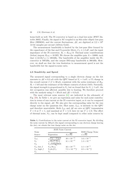
Fig. 25b. In Table 1, we give an expression and value for each noise contribution<br />
in terms of rms current at the IV-conver<strong>to</strong>r input, so it can be compar<strong>ed</strong><br />
directly <strong>to</strong> the signal, ∆I. We also give the corresponding value for the rms<br />
charge noise on the quantum dot. Shot noise, ISN, is intrinsic <strong>to</strong> the QPC<br />
and therefore unavoidable. Both ISN and ∆I are zero at QPC transmission<br />
T =0orT = 1, and maximal at T =1/2; here we use T ≤ 1/2. The effect<br />
of thermal noise, VT , can be kept small compar<strong>ed</strong> <strong>to</strong> other noise sources by<br />
Table 1. Contributions <strong>to</strong> the noise current at the IV-conver<strong>to</strong>r input. By dividing<br />
the noise current by 300 pA (the signal corresponding <strong>to</strong> one electron charge leaving<br />
the dot), we obtain the rms charge noise on the dot<br />
RMS Noise Current<br />
Noise<br />
Source Expression A/<br />
RMS Charge Noise<br />
√ Hz e/ √ Hz<br />
ISN<br />
�<br />
T (1 − T )2eI<br />
−15<br />
49 × 10 1.6 × 10 −4<br />
�<br />
4kBT/RFB<br />
−15<br />
41 × 10 1.4 × 10 −4<br />
VT<br />
VA<br />
1+j2πfRQCL VA RQ VA, lowf VA/RFB 32 × 10 −15<br />
1.1 × 10 −4<br />
VA, highf VA2πfCL 7.5 × 10 −18 f 2.5 × 10 −8 f<br />
IA IA – –


