Heiss W.D. (ed.) Quantum dots.. a doorway to - tiera.ru
Heiss W.D. (ed.) Quantum dots.. a doorway to - tiera.ru
Heiss W.D. (ed.) Quantum dots.. a doorway to - tiera.ru

Create successful ePaper yourself
Turn your PDF publications into a flip-book with our unique Google optimized e-Paper software.
50 J.M. Elzerman et al.<br />
a b<br />
c<br />
200 nm<br />
500 nm<br />
200 nm<br />
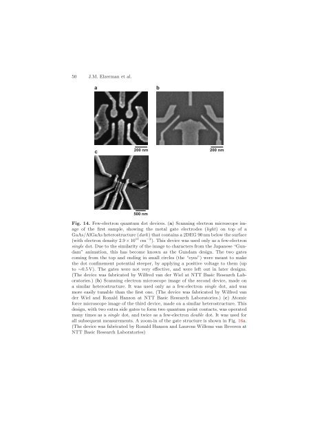
Fig. 14. Few-electron quantum dot devices. (a) Scanning electron microscope image<br />
of the first sample, showing the metal gate electrodes (light) on <strong>to</strong>p of a<br />
GaAs/AlGaAs heterost<strong>ru</strong>cture (dark) that contains a 2DEG 90 nm below the surface<br />
(with electron density 2.9 × 10 11 cm −2 ). This device was us<strong>ed</strong> only as a few-electron<br />
single dot. Due <strong>to</strong> the similarity of the image <strong>to</strong> characters from the Japanese “Gundam”<br />
animation, this has become known as the Gundam design. The two gates<br />
coming from the <strong>to</strong>p and ending in small circles (the “eyes”) were meant <strong>to</strong> make<br />
the dot confinement potential steeper, by applying a positive voltage <strong>to</strong> them (up<br />
<strong>to</strong> ∼0.5 V). The gates were not very effective, and were left out in later designs.<br />
(The device was fabricat<strong>ed</strong> by Wilfr<strong>ed</strong> van der Wiel at NTT Basic Research Labora<strong>to</strong>ries.)<br />
(b) Scanning electron microscope image of the second device, made on<br />
a similar heterost<strong>ru</strong>cture. It was us<strong>ed</strong> only as a few-electron single dot, and was<br />
more easily tunable than the first one. (The device was fabricat<strong>ed</strong> by Wilfr<strong>ed</strong> van<br />
der Wiel and Ronald Hanson at NTT Basic Research Labora<strong>to</strong>ries.) (c) A<strong>to</strong>mic<br />
force microscope image of the third device, made on a similar heterost<strong>ru</strong>cture. This<br />
design, with two extra side gates <strong>to</strong> form two quantum point contacts, was operat<strong>ed</strong><br />
many times as a single dot, and twice as a few-electron double dot. It was us<strong>ed</strong> for<br />
all subsequent measurements. A zoom-in of the gate st<strong>ru</strong>cture is shown in Fig. 16a.<br />
(The device was fabricat<strong>ed</strong> by Ronald Hanson and Laurens Willems van Beveren at<br />
NTT Basic Research Labora<strong>to</strong>ries)