Heiss W.D. (ed.) Quantum dots.. a doorway to - tiera.ru
Heiss W.D. (ed.) Quantum dots.. a doorway to - tiera.ru
Heiss W.D. (ed.) Quantum dots.. a doorway to - tiera.ru

You also want an ePaper? Increase the reach of your titles
YUMPU automatically turns print PDFs into web optimized ePapers that Google loves.
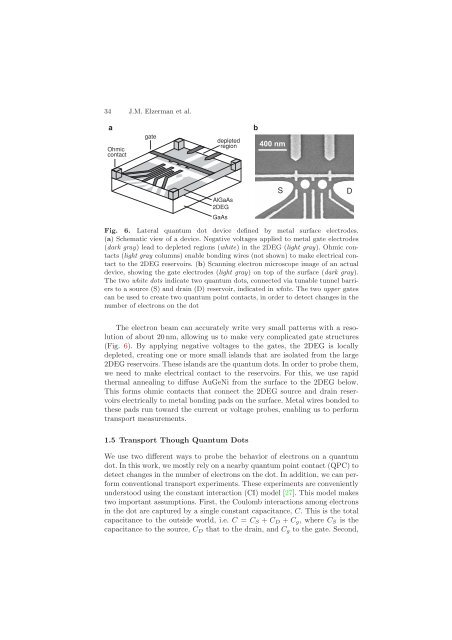
34 J.M. Elzerman et al.<br />
a<br />
Ohmic<br />
contact<br />
gate<br />
deplet<strong>ed</strong><br />
region<br />
AlGaAs<br />
2DEG<br />
GaAs<br />
b<br />
400 nm<br />
Fig. 6. Lateral quantum dot device defin<strong>ed</strong> by metal surface electrodes.<br />
(a) Schematic view of a device. Negative voltages appli<strong>ed</strong> <strong>to</strong> metal gate electrodes<br />
(dark gray) lead <strong>to</strong> deplet<strong>ed</strong> regions (white) inthe2DEG(light gray). Ohmic contacts<br />
(light gray columns) enable bonding wires (not shown) <strong>to</strong> make electrical contact<br />
<strong>to</strong> the 2DEG reservoirs. (b) Scanning electron microscope image of an actual<br />
device, showing the gate electrodes (light gray) on <strong>to</strong>p of the surface (dark gray).<br />
The two white <strong>dots</strong> indicate two quantum <strong>dots</strong>, connect<strong>ed</strong> via tunable tunnel barriers<br />
<strong>to</strong> a source (S) and drain (D) reservoir, indicat<strong>ed</strong> in white. Thetwoupper gates<br />
can be us<strong>ed</strong> <strong>to</strong> create two quantum point contacts, in order <strong>to</strong> detect changes in the<br />
number of electrons on the dot<br />
The electron beam can accurately write very small patterns with a resolution<br />
of about 20 nm, allowing us <strong>to</strong> make very complicat<strong>ed</strong> gate st<strong>ru</strong>ctures<br />
(Fig. 6). By applying negative voltages <strong>to</strong> the gates, the 2DEG is locally<br />
deplet<strong>ed</strong>, creating one or more small islands that are isolat<strong>ed</strong> from the large<br />
2DEG reservoirs. These islands are the quantum <strong>dots</strong>. In order <strong>to</strong> probe them,<br />
we ne<strong>ed</strong> <strong>to</strong> make electrical contact <strong>to</strong> the reservoirs. For this, we use rapid<br />
thermal annealing <strong>to</strong> diffuse AuGeNi from the surface <strong>to</strong> the 2DEG below.<br />
This forms ohmic contacts that connect the 2DEG source and drain reservoirs<br />
electrically <strong>to</strong> metal bonding pads on the surface. Metal wires bond<strong>ed</strong> <strong>to</strong><br />
these pads <strong>ru</strong>n <strong>to</strong>ward the current or voltage probes, enabling us <strong>to</strong> perform<br />
transport measurements.<br />
1.5 Transport Though <strong>Quantum</strong> Dots<br />
We use two different ways <strong>to</strong> probe the behavior of electrons on a quantum<br />
dot. In this work, we mostly rely on a nearby quantum point contact (QPC) <strong>to</strong><br />
detect changes in the number of electrons on the dot. In addition, we can perform<br />
conventional transport experiments. These experiments are conveniently<br />
unders<strong>to</strong>od using the constant interaction (CI) model [27]. This model makes<br />
two important assumptions. First, the Coulomb interactions among electrons<br />
in the dot are captur<strong>ed</strong> by a single constant capacitance, C. This is the <strong>to</strong>tal<br />
capacitance <strong>to</strong> the outside world, i.e. C = CS + CD + Cg, where CS is the<br />
capacitance <strong>to</strong> the source, CD that <strong>to</strong> the drain, and Cg <strong>to</strong> the gate. Second,<br />
S<br />
D