

The Impact of Dennard's Scaling Theory - IEEE
The Impact of Dennard's Scaling Theory - IEEE
The Impact of Dennard's Scaling Theory - IEEE
- TAGS
- scaling
- www.ieee.org

You also want an ePaper? Increase the reach of your titles
YUMPU automatically turns print PDFs into web optimized ePapers that Google loves.
RESEARCH HIGHLIGHTS<br />
for 10-mm Uninterrupted RC-Limited Global On-<br />
Chip Interconnects”, <strong>IEEE</strong> Journal <strong>of</strong> Solid State<br />
Circuits, Vol. 41, No. 1, pp. 297- 306, Jan. 2006.<br />
[8] J.H.R. Schrader, E.A.M. Klumperink, J.L. Visschers,<br />
B. Nauta, “Pulse-Width Modulation Pre<br />
Emphasis applied in a Wireline Transmitter,<br />
achieving 33dB Loss Compensation at 5-Gb/s in<br />
About the Author<br />
Bram Nauta was born in Hengelo,<br />
<strong>The</strong> Netherlands. In 1987 he<br />
received the M.Sc degree (cum<br />
laude) in electrical engineering from<br />
the University <strong>of</strong> Twente, Enschede,<br />
<strong>The</strong> Netherlands. In 1991 he<br />
received the Ph.D. degree from the<br />
same university on the subject <strong>of</strong><br />
analog CMOS filters for very high frequencies.<br />
In 1991 he joined the Mixed-Signal Circuits and<br />
Systems Department <strong>of</strong> Philips Research, Eindhoven<br />
the Netherlands, where he worked on high speed AD<br />
converters and analog key modules. In 1998 he<br />
returned to the University <strong>of</strong> Twente, as full pr<strong>of</strong>essor<br />
heading the IC Design group, which is part <strong>of</strong> the<br />
Corrections continued from page 4<br />
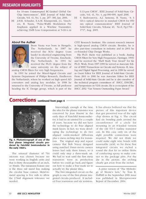
Fig. 4. Photomicrograph <strong>of</strong> one <strong>of</strong> the<br />
first planar integrated circuits produced<br />
by Fairchild Semiconductor in<br />
the early 1960’s.<br />
<strong>The</strong> unusual diameter <strong>of</strong> 764<br />
microns was chosen because we<br />
were working in English units and<br />
that is thirty thousandths <strong>of</strong> an inch,<br />
or 30mils. <strong>The</strong> minimum feature size<br />
is the three mil metal line making<br />
the circular base contact. Metal-tometal<br />
spacing is five mils to allow<br />
the 2.5mil alignment tolerance we<br />
needed.<br />
Interestingly enough at the time<br />
the idea for the planar transistor was<br />
conceived by Jean Hoerni in the<br />
early days <strong>of</strong> Fairchild Semiconductor,<br />
it had to sit untried for a couple<br />
<strong>of</strong> years, because we did not have<br />
the technology to do four aligned<br />
mask layers. In fact, we were developing<br />
the technology to do two<br />
aligned oxide-masked diffusions<br />
plus a mesa etching step for transistors.<br />
<strong>The</strong> original step and repeat<br />
camera that Bob Noyce designed<br />
using matched 16mm movie camera<br />
lenses had only three lenses, so it<br />
could only step a three-mask set.<br />
We had to wait until the first mesa<br />
transistors were in production<br />
before we could go back and figure<br />
out how to make a four mask set to<br />
actually try the planar idea.<br />
<strong>The</strong> first integrated circuit on the<br />
graph is one <strong>of</strong> the first planar integrated<br />
circuits produced. It included<br />
four transistors and six resistors.<br />
0.13-μm CMOS”, <strong>IEEE</strong> Journal <strong>of</strong> Solid-State Circuits,<br />
Vol. 41, No. 4, pp.990-999, April 2006.<br />
[9] S. Radovanovic, A.J. Annema, B. Nauta, “A 3<br />
Gb/s optical detector in standard CMOS for 850<br />
nm optical communication” <strong>IEEE</strong> Journal <strong>of</strong><br />
Solid-State Circuits, Volume 40, No.8, Pg:1706 -<br />
1717, Aug. 2005.<br />
CTIT Research Institute. His current research interest<br />
is high-speed analog CMOS circuits. Besides, he is<br />
also part-time consultant in industry and in 2001 he<br />
co-founded Chip Design Works.<br />
His Ph.D. thesis was published as a book: Analog<br />
CMOS Filters for Very High Frequencies, (Springer, 1993)<br />
and he received the “Shell Study Tour Award” for his<br />
Ph.D. Work. From 1997-1999 he served as Associate Editor<br />
<strong>of</strong> <strong>IEEE</strong> Transactions on Circuits and Systems -II; Analog<br />
and Digital Signal Processing, and in 1998 he served<br />
as Guest Editor for <strong>IEEE</strong> Journal <strong>of</strong> Solid-State Circuits.<br />
From 2001 to 2006 he was Associate Editor for <strong>IEEE</strong><br />
Journal <strong>of</strong> Solid-State Circuits and he is also member <strong>of</strong><br />
the technical program committees <strong>of</strong> ISSCC, ESSCIRC,<br />
and Symposium on VLSI circuits. He is co-recipient <strong>of</strong> the<br />
ISSCC 2002 “Van Vessem Outstanding Paper Award.”<br />
It has always bothered me that the<br />
picture <strong>of</strong> this important device<br />
that got preserved was <strong>of</strong> the ugly<br />
chip shown in Fig. 4. <strong>The</strong> circuit<br />
had six bonding pads around the<br />
circumference <strong>of</strong> a circle for<br />
mounting in an 8-leaded version<br />
<strong>of</strong> the old TO-5 outline transistor<br />
can. In this case only six <strong>of</strong> the<br />
eight possible connections were<br />
required. We did not think we<br />
could make eight wire bonds with<br />
reasonable yield, so for these first<br />
integrated circuits we etched a<br />
round die that let us utilize blobs<br />
<strong>of</strong> conducting epoxy to make contact<br />
to the package pins. For the<br />
die in the picture, the etching<br />
clearly got away from the etcher.<br />
A prior version <strong>of</strong> “<strong>The</strong> Mythology<br />
<strong>of</strong> Moore’s Law,” by Tom R.<br />
Halfhill in the September 2006 issue<br />
was published in Microprocessor<br />
Report <strong>of</strong> December, 2004.<br />
10 <strong>IEEE</strong> SSCS NEWSLETTER Winter 2007

