

The Impact of Dennard's Scaling Theory - IEEE
The Impact of Dennard's Scaling Theory - IEEE
The Impact of Dennard's Scaling Theory - IEEE
- TAGS
- scaling
- www.ieee.org

Create successful ePaper yourself
Turn your PDF publications into a flip-book with our unique Google optimized e-Paper software.
will have their capacitances reduced by a factor <strong>of</strong> κ.<br />
This occurs because <strong>of</strong> the reduction by κ 2 in the area<br />
<strong>of</strong> these components, which is partially cancelled by<br />
the decrease in the electrode spacing by κ due to<br />
thinner insulating films and reduced depletion layer<br />
widths. <strong>The</strong>se reduced capacitances are driven by the<br />
unchanged device resistances V /I giving decreased<br />
transition times with a resultant reduction in the delay<br />
time <strong>of</strong> each circuit by a factor <strong>of</strong> κ. <strong>The</strong> power dissipation<br />
<strong>of</strong> each circuit is reduced by κ 2 due to the<br />
reduced voltage and current levels, so the powerdelay<br />
product is improved by κ 3 . Since the area <strong>of</strong> a<br />
given device or circuit is also reduced by κ 2 , the<br />
power density remains constant. Thus, even if many<br />
more circuits are placed on a given integrated circuit<br />
chip, the cooling problem is essentially unchanged.<br />
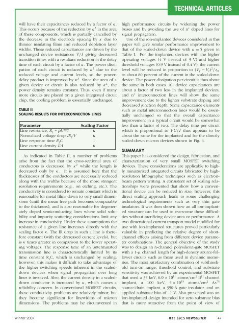
TABLE II<br />
SCALING RESULTS FOR INTERCONNECTION LINES<br />
Parameter <strong>Scaling</strong> Factor<br />
Line resistance, R L = ρL/Wt κ<br />
Normalized voltage drop IR L /V κ<br />
Line response time R L C l<br />
Line current density I/A κ<br />
As indicated in Table II, a number <strong>of</strong> problems<br />
arise from the fact that the cross-sectional area <strong>of</strong><br />
conductors is decreased by κ 2 while the length is<br />
decreased only by κ. It is assumed here that the<br />
thicknesses <strong>of</strong> the conductors are necessarily reduced<br />
along with the widths because <strong>of</strong> the more stringent<br />
resolution requirements (e.g., on etching, etc.). <strong>The</strong><br />
conductivity is considered to remain constant which is<br />
reasonable for metal films down to very small dimensions<br />
(until the mean free path becomes comparable<br />
to the thickness), and is also reasonable for degenerately<br />
doped semiconducting lines where solid solubility<br />
and impurity scattering considerations limit any<br />
increase in conductivity. Under these assumptions the<br />
resistance <strong>of</strong> a given line increases directly with the<br />
scaling factor κ. <strong>The</strong> IR drop in such a line is therefore<br />
constant (with the decreased current levels), but<br />
is κ times greater in comparison to the lower operating<br />
voltages. <strong>The</strong> response time <strong>of</strong> an unterminated<br />
transmission line is characteristically limited by its<br />
time constant R L C, which is unchanged by scaling;<br />
however, this makes it difficult to take advantage <strong>of</strong><br />
the higher switching speeds inherent in the scaleddown<br />
devices when signal propagation over long<br />
lines is involved. Also, the current density in a scaleddown<br />
conductor is increased by κ, which causes a<br />
reliability concern. In conventional MOSFET circuits,<br />
these conductivity problems are relatively minor, but<br />
they become significant for linewidths <strong>of</strong> micron<br />
dimensions. <strong>The</strong> problems may he circumvented in<br />
TECHNICAL ARTICLES<br />
high performance circuits by widening the power<br />
buses and by avoiding the use <strong>of</strong> n + doped lines for<br />
signal propagation.<br />
Use <strong>of</strong> the ion-implanted devices considered in this<br />
paper will give similar performance improvement to<br />
that <strong>of</strong> the scaled-down device with κ = 5 given in<br />
Table I. For the implanted devices with the higher<br />
operating voltages (4 V instead <strong>of</strong> 3 V) and higher<br />
threshold voltages (0.9 V instead <strong>of</strong> 0.4 V), the current<br />
level will be reduced in proportion to (Vg − Vt) 2 /tox<br />
to about 80 percent <strong>of</strong> the current in the scaled-down<br />
device. <strong>The</strong> power dissipation per circuit is thus about<br />
the same in both cases. All device capacitances are<br />
about a factor <strong>of</strong> two less in the implanted devices,<br />
and n + interconnection lines will show the same<br />
improvement due to the lighter substrate doping and<br />
decreased junction depth. Some capacitance elements<br />
such as metal interconnection lines would be essentially<br />
unchanged so that the overall capacitance<br />
improvement in a typical circuit would be somewhat<br />
less than a factor <strong>of</strong> two. <strong>The</strong> delay time per circuit<br />
which is proportional to VC/I thus appears to be<br />
about the same for the implanted and for the directly<br />
scaled-down micron devices shown in Fig. 4.<br />
SUMMARY<br />
This paper has considered the design, fabrication, and<br />
characterization <strong>of</strong> very small MOSFET switching<br />
devices. <strong>The</strong>se considerations are applicable to highly<br />
miniaturized integrated circuits fabricated by highresolution<br />
lithographic techniques such as electronbeam<br />
pattern writing. A consistent set <strong>of</strong> scaling relationships<br />
were presented that show how a conventional<br />
device can be reduced in size; however, this<br />
direct scaling approach leads to some challenging<br />
technological requirements such as very thin gate<br />
insulators. It was then shown how an all ion-implanted<br />
structure can be used to overcome these difficulties<br />
without sacrificing device area or performance. A<br />
two-dimensional current transport model modified for<br />
use with ion-implanted structures proved particularly<br />
valuable in predicting the relative degree <strong>of</strong> shortchannel<br />
effects arising from different device parameter<br />
combinations. <strong>The</strong> general objective <strong>of</strong> the study<br />
was to design an n-channel polysilicon-gate MOSFET<br />
with a 1-μ channel length for high-density source-follower<br />
circuits such as those used in dynamic memories.<br />
<strong>The</strong> most satisfactory combination <strong>of</strong> subthreshold<br />
turn-on range, threshold control, and substrate<br />
sensitivity was achieved by an experimental MOSFET<br />
that used a 35 keV, 6.0 × 10 11 atoms/cm 2 B 11 channel<br />
implant, a 100 keV, 4 × 10 15 atoms/cm 2 As 75<br />
source/drain implant, a 350-Å gate insulator, and an<br />
applied substrate bias <strong>of</strong> –1 V. Also presented was an<br />
ion-implanted design intended for zero substrate bias<br />
that is more attractive from the point <strong>of</strong> view <strong>of</strong><br />
Winter 2007 <strong>IEEE</strong> SSCS NEWSLETTER 47

