

The Impact of Dennard's Scaling Theory - IEEE
The Impact of Dennard's Scaling Theory - IEEE
The Impact of Dennard's Scaling Theory - IEEE
- TAGS
- scaling
- www.ieee.org

Create successful ePaper yourself
Turn your PDF publications into a flip-book with our unique Google optimized e-Paper software.
processing, the boron is redistributed as shown by the<br />
heavier dashed line. <strong>The</strong>se predicted pr<strong>of</strong>iles were<br />
obtained using a computer program developed by F.<br />
F. Morehead <strong>of</strong> our laboratories. <strong>The</strong> program<br />
assumes that boron atoms diffusing in the silicon<br />
reflect from the silicon-oxide interface and thereby<br />
raise the surface concentration. For modeling purposes<br />
it is convenient to use a simple, idealized, stepfunction<br />
representation <strong>of</strong> the doping pr<strong>of</strong>ile, as<br />
shown by the solid line in Fig. 5. <strong>The</strong> step pr<strong>of</strong>ile<br />
approximates the final predicted pr<strong>of</strong>ile rather well<br />
and <strong>of</strong>fers the advantage that it can be described by a<br />
few simple parameters. <strong>The</strong> three pr<strong>of</strong>iles shown in<br />
Fig. 5 all have the same active dose.<br />
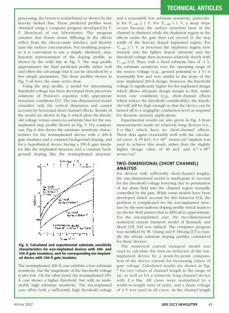
Using the step pr<strong>of</strong>ile, a model for determining<br />
threshold voltage has been developed from piecewise<br />
solutions <strong>of</strong> Poisson’s equation with appropriate<br />
boundary conditions [11]. <strong>The</strong> one-dimensional model<br />
considers only the vertical dimension and cannot<br />
account for horizontal short-channel effects. Results <strong>of</strong><br />
the model are shown in Fig, 6 which plots the threshold<br />
voltage versus source-to-substrate bias for the ionimplanted<br />
step pr<strong>of</strong>ile shown in Fig. 5. For comparison,<br />
Fig. 6 also shows the substrate sensitivity characteristics<br />
for the nonimplanted device with a 200-Å<br />
gate insulator and a constant background doping, and<br />
for a hypothetical device having a 350-Å gate insulator<br />
like the implanted structure and a constant background<br />
doping like the nonimplanted structure.<br />
Fig. 6. Calculated and experimental substrate sensitivity<br />
characteristics for non-implanted devices with 200- and<br />
350-Å gate insulators, and for corresponding ion-implanted<br />
device with 350-Å gate insulator.<br />
<strong>The</strong> nonimplanted 200-Å case exhibits a low substrate<br />
sensitivity, but the magnitude <strong>of</strong> the threshold voltage<br />
is also low. On the other hand, the nonimplanted 350-<br />
Å case shows a higher threshold, but with an undesirably<br />
high substrate sensitivity. <strong>The</strong> ion-implanted<br />
case <strong>of</strong>fers both a sufficiently high threshold voltage<br />
TECHNICAL ARTICLES<br />
and a reasonably low substrate sensitivity, particularly<br />
for Vs−sub ≥ 1 V. For Vs−sub < 1 V, a steep slope<br />
occurs because the surface inversion layer in the<br />
channel is obtained while the depletion region in the<br />
silicon under the gate does not exceed D, the step<br />
width <strong>of</strong> the heavier doped implanted region. For<br />
Vs−sub ≥ 1 V, at inversion the depletion region now<br />
extends into the lighter doped substrate and the<br />
threshold voltage then increases relatively slowly with<br />
Vs−sub [11]. Thus, with a fixed substrate bias <strong>of</strong> -1 V,<br />
the substrate sensitivity over the operating range <strong>of</strong><br />
the source voltage (e.g., ground potential to 4 V) is<br />
reasonably low and very similar to the slope <strong>of</strong> the<br />
non- implanted 200-Å design. However, the threshold<br />
voltage is significantly higher for the implanted design<br />
which allows adequate design margin so that, under<br />
worst case conditions (e.g., short-channel effects<br />
which reduce the threshold considerably), the threshold<br />
will still be high enough so that the device can be<br />
turned <strong>of</strong>f to a negligible conduction level as required<br />
for dynamic memory applications.<br />
Experimental results are also given in Fig. 6 from<br />
measurements made on relatively long devices (i.e.,<br />
L = 10μ) which have no short-channel effects.<br />
<strong>The</strong>se data agree reasonably well with the calculated<br />
curve. A 35 keV, 6 × 10 11 atoms/cm 2 implant was<br />
used to achieve this result, rather than the slightly<br />
higher design value <strong>of</strong> 40 keV and 6.7 × 10 11<br />
atoms/cm 2 .<br />
TWO-DIMENSIONAL (SHORT CHANNEL)<br />
ANALYSIS<br />
For devices with sufficiently short-channel lengths,<br />
the one-dimensional model is inadequate to account<br />
for the threshold voltage lowering due to penetration<br />
<strong>of</strong> the drain field into the channel region normally<br />
controlled by the gate. While some models have been<br />
developed which account for this behavior [14], the<br />
problem is complicated for the ion-implanted structure<br />
by the non-uniform doping pr<strong>of</strong>ile which leads to<br />
an electric field pattern that is difficult to approximate.<br />
For the ion-implanted case, the two-dimensional<br />
numerical current transport model <strong>of</strong> Kennedy and<br />
Mock [15], [16] was utilized. <strong>The</strong> computer program<br />
was modified by W. Chang and P. Hwang [17] to handle<br />
the abrupt substrate doping pr<strong>of</strong>iles considered<br />
for these devices.<br />
<strong>The</strong> numerical current transport model was<br />
used to calculate the turn-on behavior <strong>of</strong> the ionimplanted<br />
device by a point-by-point computation<br />
<strong>of</strong> the device current for increasing values <strong>of</strong><br />
gate voltage. Calculated results are shown in Fig.<br />
7 for two values <strong>of</strong> channel length in the range <strong>of</strong><br />
1μ, as well as for a relatively long-channel device<br />
with L = 10μ. All cases were normalized to a<br />
width-to-length ratio <strong>of</strong> unity, and a drain voltage<br />
<strong>of</strong> 4 V was used in all cases. As the channel length<br />
Winter 2007 <strong>IEEE</strong> SSCS NEWSLETTER 43

