

The Impact of Dennard's Scaling Theory - IEEE
The Impact of Dennard's Scaling Theory - IEEE
The Impact of Dennard's Scaling Theory - IEEE
- TAGS
- scaling
- www.ieee.org

Create successful ePaper yourself
Turn your PDF publications into a flip-book with our unique Google optimized e-Paper software.
TECHNICAL ARTICLES<br />
However, a typical MOSFET in production in the<br />
early 1970’s had a gate oxide <strong>of</strong> about 100 nm in<br />
thickness, a channel length <strong>of</strong> about 5 μm, and a<br />
power supply voltage <strong>of</strong> 5 V or larger. As explained<br />
in a paragraph below, the performance <strong>of</strong> these highvoltage<br />
MOSFET circuits was simply much too inferior<br />
compared to the performance <strong>of</strong> silicon bipolar circuits.<br />
Bipolar was the high-performance technology,<br />
the backbone <strong>of</strong> computers and high-performance<br />
electronics, while MOSFET was the low-cost technology<br />
for applications where performance was not<br />
required.<br />
<strong>The</strong> benefit <strong>of</strong> applying the scaling theory to MOS-<br />
FET technology, especially to CMOS technology,<br />
seemed obvious and exciting. If we just follow the<br />
rules and scale the CMOS devices by a factor <strong>of</strong> ten,<br />
the resulting circuits will be ten times faster. For more<br />
than two decades following the publication <strong>of</strong> the<br />
MOSFET scaling theory, CMOS engineers focused<br />
much <strong>of</strong> their efforts in scaling down the physical size<br />
<strong>of</strong> CMOS transistors. However, instead <strong>of</strong> scaling<br />
down the power supply voltage, they left it at 5 volts,<br />
which was the standard for practically all integrated<br />
circuits. <strong>The</strong>re was simply little or no market for integrated-circuit<br />
chips using non-standard voltages. Such<br />
constant-voltage scaling <strong>of</strong> MOSFET quickly ran into<br />
two major difficulties, namely the power density <strong>of</strong> a<br />
CMOS circuit in switching increased very rapidly by a<br />
factor <strong>of</strong> κ 2 to κ 3, and the fast increasing electric field<br />
caused hot-electron and oxide reliability problems.<br />
Power density was not much <strong>of</strong> a problem because<br />
the integration level was still relatively low so that the<br />
total chip power was readily manageable. However,<br />
device engineers had to devote much effort to develop<br />
practical techniques, such as LDD (Lightly Doped<br />
Drain) [4], in order to bring the reliability issues under<br />
control. Controlling hot-electron effects added significant<br />
cost to the CMOS chips.<br />
<strong>Scaling</strong> at constant voltage severely limited the performance<br />
potential <strong>of</strong> CMOS as well, particularly for<br />
driving long wires and driving signals <strong>of</strong>f chip. To first<br />
order, the performance for driving a capacitance load C<br />
is CV/I, where V is the voltage swing and I is the current<br />
delivered by the transistor. For bipolar circuits, V is<br />
typically about 200-400 mV for driving on chip, and<br />
about 800 mV for driving <strong>of</strong>f chip. Thus, at 5 V, the voltage<br />
swing <strong>of</strong> CMOS circuits was much too large for<br />
high-performance applications. Besides, in the late<br />
1970’s, bipolar engineers also developed a theory for<br />
scaling bipolar circuits [5] which guided the rapid<br />
development <strong>of</strong> faster and lower-power bipolar circuits.<br />
For more than twenty years after the MOSFET theory<br />
was published, CMOS remained a low-cost technology<br />
limited to applications where performance was not an<br />
important factor. When performance was needed,<br />
scaled advanced bipolar technology was used.<br />
<strong>The</strong> opportunity for scaled CMOS to break into<br />
high-end applications came when the industry<br />
worked together to established voltage standards<br />
below 5 volt. Once it was recognized that CMOS at<br />
less than 5 V could be accepted by the market, engineers<br />
wanted to reduce CMOS voltage as fast as possible.<br />
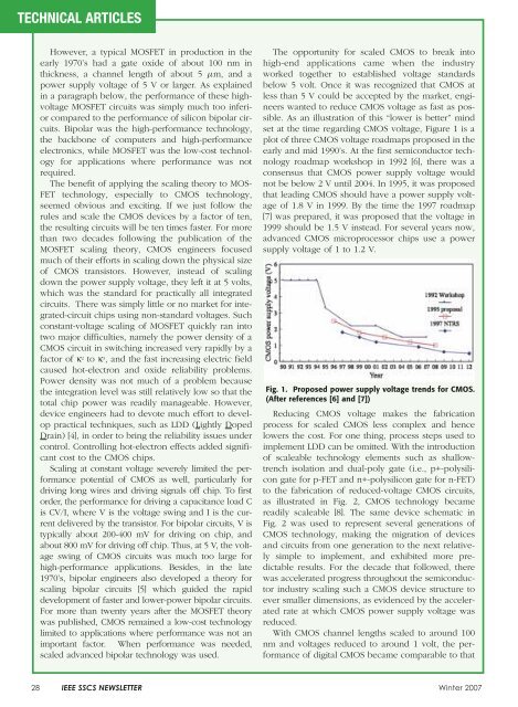
As an illustration <strong>of</strong> this “lower is better” mind<br />
set at the time regarding CMOS voltage, Figure 1 is a<br />
plot <strong>of</strong> three CMOS voltage roadmaps proposed in the<br />
early and mid 1990’s. At the first semiconductor technology<br />
roadmap workshop in 1992 [6], there was a<br />
consensus that CMOS power supply voltage would<br />
not be below 2 V until 2004. In 1995, it was proposed<br />
that leading CMOS should have a power supply voltage<br />
<strong>of</strong> 1.8 V in 1999. By the time the 1997 roadmap<br />
[7] was prepared, it was proposed that the voltage in<br />
1999 should be 1.5 V instead. For several years now,<br />
advanced CMOS microprocessor chips use a power<br />
supply voltage <strong>of</strong> 1 to 1.2 V.<br />
Fig. 1. Proposed power supply voltage trends for CMOS.<br />
(After references [6] and [7])<br />
Reducing CMOS voltage makes the fabrication<br />
process for scaled CMOS less complex and hence<br />
lowers the cost. For one thing, process steps used to<br />
implement LDD can be omitted. With the introduction<br />
<strong>of</strong> scaleable technology elements such as shallowtrench<br />
isolation and dual-poly gate (i.e., p+-polysilicon<br />
gate for p-FET and n+-polysilicon gate for n-FET)<br />
to the fabrication <strong>of</strong> reduced-voltage CMOS circuits,<br />
as illustrated in Fig. 2, CMOS technology became<br />
readily scaleable [8]. <strong>The</strong> same device schematic in<br />
Fig. 2 was used to represent several generations <strong>of</strong><br />
CMOS technology, making the migration <strong>of</strong> devices<br />
and circuits from one generation to the next relatively<br />
simple to implement, and exhibited more predictable<br />
results. For the decade that followed, there<br />
was accelerated progress throughout the semiconductor<br />
industry scaling such a CMOS device structure to<br />
ever smaller dimensions, as evidenced by the accelerated<br />
rate at which CMOS power supply voltage was<br />
reduced.<br />
With CMOS channel lengths scaled to around 100<br />
nm and voltages reduced to around 1 volt, the performance<br />
<strong>of</strong> digital CMOS became comparable to that<br />
28 <strong>IEEE</strong> SSCS NEWSLETTER Winter 2007

