

The Impact of Dennard's Scaling Theory - IEEE
The Impact of Dennard's Scaling Theory - IEEE
The Impact of Dennard's Scaling Theory - IEEE
- TAGS
- scaling
- www.ieee.org

Create successful ePaper yourself
Turn your PDF publications into a flip-book with our unique Google optimized e-Paper software.
TECHNICAL ARTICLES<br />
threshold control but suffers from an increased subthreshold<br />
turn-on range. Finally the sizable performance<br />
improvement expected from using very small<br />
MOSFET’s in integrated circuits <strong>of</strong> comparably small<br />
dimensions was projected.<br />
APPENDIX<br />
EXPERIMENTAL DETERMINATION OF<br />
CHANNEL LENGTH<br />
A technique for determining the effective electrical<br />
channel length L for very small MOSFET’s from experimental<br />
data is described here. <strong>The</strong> technique is based<br />
on the observation that<br />
WRchan = Lρchan<br />
(A1)<br />
where Rchan is the channel resistance, and ρchan the<br />
sheet resistance <strong>of</strong> the channel. For a fixed value <strong>of</strong><br />
Vg − Vt > 0, and with the device turned on in the<br />
below-pinch<strong>of</strong>f region, the channel sheet resistance is<br />
relatively independent <strong>of</strong> L. <strong>The</strong>n, a plot <strong>of</strong> WRchan<br />
versus L mask will intercept the L mask axis at �L<br />
because �L = L mask − L , where �L is the processing<br />
reduction in the mask dimension due to exposure and<br />
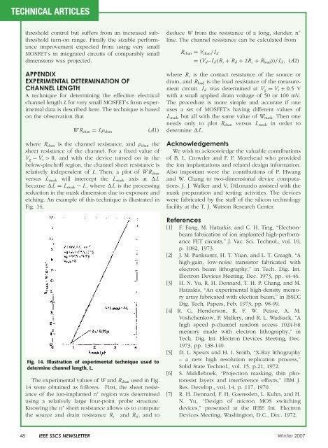
etching. An example <strong>of</strong> this technique is illustrated in<br />
Fig. 14.<br />
Fig. 14. lllustration <strong>of</strong> experimental technique used to<br />
determine channel length, L.<br />
<strong>The</strong> experimental values <strong>of</strong> W and Rchan used in Fig.<br />
14 were obtained as follows. First, the sheet resistance<br />
<strong>of</strong> the ion-implanted n + region was determined<br />
using a relatively large four-point probe structure.<br />
Knowing the n + sheet resistance allows us to compute<br />
the source and drain resistance R s and Rd , and to<br />
deduce W from the resistance <strong>of</strong> a long, slender, n +<br />
line. <strong>The</strong> channel resistance can be calculated from<br />
Rchan = Vchan/Id<br />
= (Vd –Id (R s + Rd + 2Rc + Rload))/Id , (A2)<br />
where Rc is the contact resistance <strong>of</strong> the source or<br />
drain, and Rload is the load resistance <strong>of</strong> the measurement<br />
circuit. Id was determined at Vg = Vt + 0.5 V<br />
with a small applied drain voltage <strong>of</strong> 50 or 100 mV.<br />
<strong>The</strong> procedure is more simple and accurate if one<br />
uses a set <strong>of</strong> MOSFET’s having different values <strong>of</strong><br />
L mask but all with the same value <strong>of</strong> Wmask. <strong>The</strong>n one<br />
needs only to plot Rchan versus L mask in order to<br />
determine �L.<br />
Acknowledgements<br />
We wish to acknowledge the valuable contributions<br />
<strong>of</strong> B. L. Crowder and F. F. Morehead who provided<br />
the ion implantations and related design information.<br />
Also important were the contributions <strong>of</strong> P. Hwang<br />
and W. Chang to two-dimensional device computations.<br />
J. J. Walker and V. DiLonardo assisted with the<br />
mask preparation and testing activities. <strong>The</strong> devices<br />
were fabricated by the staff <strong>of</strong> the silicon technology<br />
facility at the T. J. Watson Research Center.<br />
References<br />
[1] F. Fang, M. Hatzakis, and C. H. Ting, “Electronbeam<br />
fabrication <strong>of</strong> ion implanted high-performance<br />
FET circuits,” J. Vac. Sci. Technol., vol. 10,<br />
p. 1082, 1973.<br />
[2] J. M. Pankrantz, H. T. Yuan, and L. T. Creagh, “A<br />
high-gain, low-noise transistor fabricated with<br />
electron beam lithography,” in Tech. Dig. Int.<br />
Electron Devices Meeting, Dec. 1973, pp. 44-46.<br />
[3] H. N. Yu, R. H. Dennard, T. H. P. Chang, and M.<br />
Hatzakis, “An experimental high-density memory<br />
array fabricated with election beam,” in ISSCC<br />
Dig. Tech. Papers, Feb. 1973, pp. 98-99.<br />
[4] R. C, Henderson, R. F. W. Pease, A. M.<br />
Voshchenkow, P. Mallery, and R. L. Wadsack, “A<br />
high speed p-channel random access 1024-bit<br />
memory made with electron lithography,” in<br />
Tech. Dig. Int. Electron Devices Meeting, Dec.<br />
1973, pp. 138-140.<br />
[5] D. L. Spears and H. I. Smith, “X-Ray lithography<br />
– a new high resolution replication process,”<br />
Solid State Technol., vol. 15, p.21, 1972.<br />
[6] S. Middlehoek, “Projection masking, thin photoresist<br />
layers and interference effects,” IBM J.<br />
Res. Develop., vol. 14, p. 117, 1970.<br />
[7] R. H. Dennard, F. H, Gaensslen, L. Kuhn, and H.<br />
N. Yu, “Design <strong>of</strong> micron MOS switching<br />
devices,” presented at the <strong>IEEE</strong> Int. Electron<br />
Devices Meeting, Washington, D.C., Dec. 1972.<br />
48 <strong>IEEE</strong> SSCS NEWSLETTER Winter 2007

