

The Impact of Dennard's Scaling Theory - IEEE
The Impact of Dennard's Scaling Theory - IEEE
The Impact of Dennard's Scaling Theory - IEEE
- TAGS
- scaling
- www.ieee.org

Create successful ePaper yourself
Turn your PDF publications into a flip-book with our unique Google optimized e-Paper software.
TECHNICAL ARTICLES<br />
[13] “CMOS scaling for high performance and low<br />
power – <strong>The</strong> Next Ten Years”; B. Davari, R. H.<br />
Dennard, and G. G. Shahidi; Proceedings <strong>of</strong> the<br />
<strong>IEEE</strong>, Vol. 83, No. 4, pp. 595-606, April, 1995. Earlier<br />
version published in Nikkei Microelectronics, pp.<br />
144-1`54, September 1994.<br />
[14] “MOSFET miniaturization – From one micron to the<br />
limits”; R. H. Dennard and M. R. Wordeman; Physica<br />
B + C, vol. 129, pp. 3-15, 1985.<br />
[15] “A high performance 0.25 μm CMOS technology”;<br />
B. Davari, W. H. Chang, M. R. Wordeman, C. S. Oh,<br />
Y. Taur, K. E. Petrillo, D. Moy, J. J. Bucchignano, H.<br />
Y. Ng, M. G. Rosenfield, F. J. Hohn, M. D. Rodriguez;<br />
IEDM Tech. Dig., pp. 56 - 59, December 1988.<br />
[16] Research Highlights with focus on Moore’s Law;<br />
<strong>IEEE</strong> Solid-State Circuits Society Newsletter, vol. 20,<br />
no. 3, September 2006.<br />
[17] “Fabrication <strong>of</strong> high-performance LDDFET's with<br />
oxide sidewall-spacer technology”; Paul J. Tsang,<br />
Seiki Ogura, William W. Walker, Joseph F. Shepard,<br />
Dale L. Critchlow; <strong>IEEE</strong> Trans. Electron Devices, vol.<br />
29, pp. 590 - 596, April 1982.<br />
[18] “Possibilities <strong>of</strong> CMOS Mainframe and its <strong>Impact</strong> on<br />
Technology R&D”: A. Masaki, Symposium on VLSI<br />
Technology, May 28-30, 1991, pp. 1-4.<br />
About the Author<br />
Dale Critchlow is a retired electrical<br />
engineer with 35 years experience<br />
at IBM and 15 years in academia.<br />
He received his Ph.D. in Electrical<br />
Engineering from Carnegie Institute<br />
<strong>of</strong> Technology in 1956. After teaching<br />
at CIT for two years, he joined<br />
IBM Research. He became one the<br />
early members <strong>of</strong> the NMOS MOSFET project in the<br />
T. J. Watson Research Center in 1964, where he<br />
managed the MOSFET device and circuit design<br />
work through 1976. Next he transferred to the IBM<br />
Components Division, first in East Fishkill, NY, and<br />
then in Essex Junction, VT where he managed a<br />
group responsible for the advanced development <strong>of</strong><br />
MOSFET logic and memory technologies. He retired<br />
from IBM in 1993 and was faculty member at the<br />
University <strong>of</strong> Vermont until 2005. He has active in<br />
<strong>IEEE</strong> activities and has published a number <strong>of</strong><br />
papers and patents.<br />
Dr. Critchlow is a Life Fellow <strong>of</strong> the Institute <strong>of</strong><br />
Electrical and Electronic Engineers, an IBM Fellow<br />
and a member <strong>of</strong> the National Academy <strong>of</strong><br />
Engineers.<br />
1 Ross Bassett wrote an excellent Ph.D. thesis and published a book [1] on the early history <strong>of</strong> the MOSFET technology. <strong>The</strong> appendices have a wealth <strong>of</strong><br />
authoritative historical information.<br />
2 Concurrently, B. Hoeneisen and C. Mead published a theoretical paper [5] projecting that a 0.4mm transistor with 14nm oxides and 2V operation could<br />
be built.<br />
<strong>The</strong> Business <strong>of</strong> <strong>Scaling</strong><br />
Rakesh Kumar<br />
TCX Inc., Technology Connexions<br />
San Diego, CA<br />
rakesh@tcxinc.com<br />
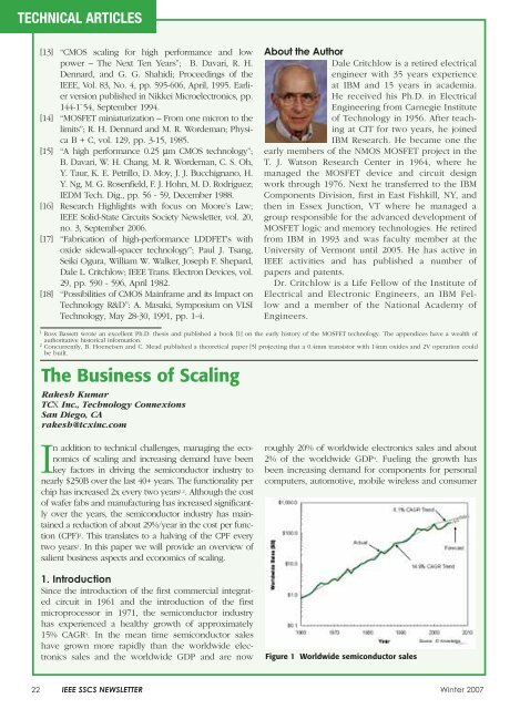
In addition to technical challenges, managing the economics<br />
<strong>of</strong> scaling and increasing demand have been<br />
key factors in driving the semiconductor industry to<br />
nearly $250B over the last 40+ years. <strong>The</strong> functionality per<br />
chip has increased 2x every two years 1,2. Although the cost<br />
<strong>of</strong> wafer fabs and manufacturing has increased significantly<br />
over the years, the semiconductor industry has maintained<br />
a reduction <strong>of</strong> about 29%/year in the cost per function<br />
(CPF) 3. This translates to a halving <strong>of</strong> the CPF every<br />
two years 1. In this paper we will provide an overview <strong>of</strong><br />
salient business aspects and economics <strong>of</strong> scaling.<br />
1. Introduction<br />
Since the introduction <strong>of</strong> the first commercial integrated<br />
circuit in 1961 and the introduction <strong>of</strong> the first<br />
microprocessor in 1971, the semiconductor industry<br />
has experienced a healthy growth <strong>of</strong> approximately<br />
15% CAGR 4. In the mean time semiconductor sales<br />
have grown more rapidly than the worldwide electronics<br />
sales and the worldwide GDP and are now<br />
roughly 20% <strong>of</strong> worldwide electronics sales and about<br />
2% <strong>of</strong> the worldwide GDP 4. Fueling the growth has<br />
been increasing demand for components for personal<br />
computers, automotive, mobile wireless and consumer<br />
Figure 1 Worldwide semiconductor sales<br />
22 <strong>IEEE</strong> SSCS NEWSLETTER Winter 2007

