

The Impact of Dennard's Scaling Theory - IEEE
The Impact of Dennard's Scaling Theory - IEEE
The Impact of Dennard's Scaling Theory - IEEE
- TAGS
- scaling
- www.ieee.org

Create successful ePaper yourself
Turn your PDF publications into a flip-book with our unique Google optimized e-Paper software.
TECHNICAL ARTICLES<br />
oxides from the audience many <strong>of</strong> whom were struggling<br />
with making reliable 100nm oxides.) This was<br />
soon followed with a 1973 IEDM paper (6) utilizing<br />
ion-implantation to allow improved scaled transistors.<br />
<strong>The</strong> paper normally considered the “scaling paper”<br />
was published in 1974 (7). In 1975 Dennard, with others,<br />
proceeded to demonstrate scaling on a complex<br />
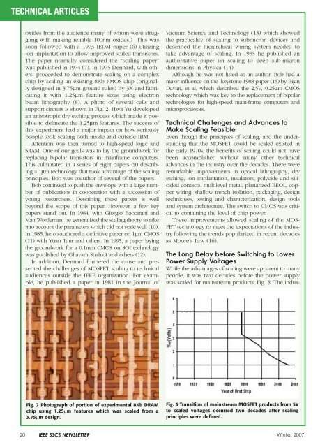
chip by scaling an existing 8Kb PMOS chip (originally<br />
designed in 3.75μm ground rules) by 3X and fabricating<br />
it with 1.25μm feature sizes using electron<br />
beam lithography (8). A photo <strong>of</strong> several cells and<br />
support circuits is shown in Fig. 2. Hwa Yu developed<br />
an anisotropic dry etching process which made it possible<br />
to delineate the 1.25μm features. <strong>The</strong> success <strong>of</strong><br />
this experiment had a major impact on how seriously<br />
people took scaling both inside and outside IBM.<br />
Attention was then turned to high-speed logic and<br />
SRAM. One <strong>of</strong> our goals was to lay the groundwork for<br />
replacing bipolar transistors in mainframe computers.<br />
This culminated in a series <strong>of</strong> eight papers (9) describing<br />
a 1μm technology that took advantage <strong>of</strong> the scaling<br />
principles. Bob was coauthor <strong>of</strong> several <strong>of</strong> the papers.<br />
Bob continued to push the envelope with a large number<br />
<strong>of</strong> publications in cooperation with a succession <strong>of</strong><br />
young researchers. Describing these papers is well<br />
beyond the scope <strong>of</strong> this paper. However, a few key<br />
papers stand out. In 1984, with Giorgio Baccarani and<br />
Matt Wordeman, he generalized the scaling theory to take<br />
into account the parameters which did not scale well (10).<br />
In 1985, he co-authored a definitive paper on 1μm CMOS<br />
(11) with Yuan Taur and others. In 1995, a paper laying<br />
the groundwork for a 0.1mm CMOS on SOI technology<br />
was published by Ghavam Shahidi and others (12).<br />
In addition, Dennard furthered the cause and presented<br />
the challenges <strong>of</strong> MOSFET scaling to technical<br />
audiences outside the <strong>IEEE</strong> organization. For example,<br />
he published a paper in 1981 in the Journal <strong>of</strong><br />
Fig. 2 Photograph <strong>of</strong> portion <strong>of</strong> experimental 8Kb DRAM<br />
chip using 1.25μm features which was scaled from a<br />
3.75μm design.<br />
Vacuum Science and Technology (13) which showed<br />
the practicality <strong>of</strong> scaling to submicron devices and<br />
described the hierarchical wiring system needed to<br />
take advantage <strong>of</strong> scaling. In 1985 he published an<br />
authoritative paper on scaling to deep sub-micron<br />
dimensions in Physica (14).<br />
Although he was not listed as an author, Bob had a<br />
major influence on the keystone 1988 paper (15) by Bijan<br />
Davari, et al, which described the 2.5V, 0.25μm CMOS<br />
technology which was key to the replacement <strong>of</strong> bipolar<br />
technologies for high-speed main-frame computers and<br />
microprocessors.<br />
Technical Challenges and Advances to<br />
Make <strong>Scaling</strong> Feasible<br />
Even though the principles <strong>of</strong> scaling, and the understanding<br />
that the MOSFET could be scaled existed in<br />
the early 1970s, the benefits <strong>of</strong> scaling could not have<br />
been accomplished without many other technical<br />
advances in the industry over the decades. <strong>The</strong>re were<br />
remarkable improvements in optical lithography, dry<br />
etching, ion implantation, insulators, polycide and silicided<br />
contacts, multilevel metal, planarized BEOL, copper<br />
wiring, shallow trench isolation, packaging, design<br />
techniques, testing and characterization, design tools<br />
and system architecture. <strong>The</strong> switch to CMOS was critical<br />
to containing the level <strong>of</strong> chip power.<br />
<strong>The</strong>se improvements allowed scaling <strong>of</strong> the MOS-<br />
FET technology to meet the expectations <strong>of</strong> the industry<br />
following the trends popularized in recent decades<br />
as Moore’s Law (16).<br />
<strong>The</strong> Long Delay before Switching to Lower<br />
Power Supply Voltages<br />
While the advantages <strong>of</strong> scaling were apparent to many<br />
people, it was two decades before the power supply<br />
was scaled for mainstream products, Fig. 3. <strong>The</strong> indus-<br />
Fig. 3 Transition <strong>of</strong> mainstream MOSFET products from 5V<br />
to scaled voltages occurred two decades after scaling<br />
principles were defined.<br />
20 <strong>IEEE</strong> SSCS NEWSLETTER Winter 2007

