

The Impact of Dennard's Scaling Theory - IEEE
The Impact of Dennard's Scaling Theory - IEEE
The Impact of Dennard's Scaling Theory - IEEE
- TAGS
- scaling
- www.ieee.org

You also want an ePaper? Increase the reach of your titles
YUMPU automatically turns print PDFs into web optimized ePapers that Google loves.
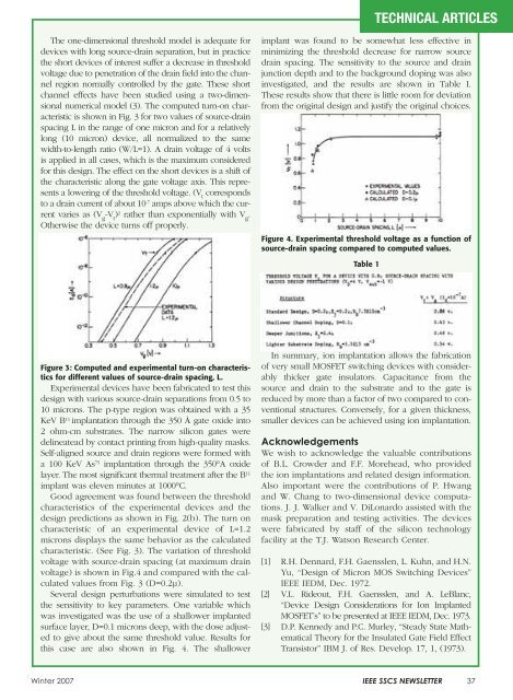
<strong>The</strong> one-dimensional threshold model is adequate for<br />
devices with long source-drain separation, but in practice<br />
the short devices <strong>of</strong> interest suffer a decrease in threshold<br />
voltage due to penetration <strong>of</strong> the drain field into the channel<br />
region normally controlled by the gate. <strong>The</strong>se short<br />
channel effects have been studied using a two-dimensional<br />
numerical model (3). <strong>The</strong> computed turn-on characteristic<br />
is shown in Fig. 3 for two values <strong>of</strong> source-drain<br />
spacing L in the range <strong>of</strong> one micron and for a relatively<br />
long (10 micron) device, all normalized to the same<br />
width-to-length ratio (W/L=1). A drain voltage <strong>of</strong> 4 volts<br />
is applied in all cases, which is the maximum considered<br />
for this design. <strong>The</strong> effect on the short devices is a shift <strong>of</strong><br />
the characteristic along the gate voltage axis. This represents<br />
a lowering <strong>of</strong> the threshold voltage. (V t corresponds<br />
to a drain current <strong>of</strong> about 10 -7 amps above which the current<br />
varies as (V g -V t ) 2 rather than exponentially with V g .<br />
Otherwise the device turns <strong>of</strong>f properly.<br />
Figure 3: Computed and experimental turn-on characteristics<br />
for different values <strong>of</strong> source-drain spacing, L.<br />
Experimental devices have been fabricated to test this<br />
design with various source-drain separations from 0.5 to<br />
10 microns. <strong>The</strong> p-type region was obtained with a 35<br />
KeV B 11 implantation through the 350 Å gate oxide into<br />
2 ohm-cm substrates. <strong>The</strong> narrow silicon gates were<br />
delineatead by contact printing from high-quality masks.<br />
Self-aligned source and drain regions were formed with<br />
a 100 KeV As 75 implantation through the 350°A oxide<br />
layer. <strong>The</strong> most significant thermal treatment after the B 11<br />
implant was eleven minutes at 1000°C.<br />
Good agreement was found between the threshold<br />
characteristics <strong>of</strong> the experimental devices and the<br />
design predictions as shown in Fig. 2(b). <strong>The</strong> turn on<br />
characteristic <strong>of</strong> an experimental device <strong>of</strong> L=1.2<br />
microns displays the same behavior as the calculated<br />
characteristic. (See Fig. 3). <strong>The</strong> variation <strong>of</strong> threshold<br />
voltage with source-drain spacing (at maximum drain<br />
voltage) is shown in Fig.4 and compared with the calculated<br />
values from Fig. 3 (D=0.2µ).<br />
Several design perturbations were simulated to test<br />
the sensitivity to key parameters. One variable which<br />
was investigated was the use <strong>of</strong> a shallower implanted<br />
surface layer, D=0.1 microns deep, with the dose adjusted<br />
to give about the same threshold value. Results for<br />
this case are also shown in Fig. 4. <strong>The</strong> shallower<br />
TECHNICAL ARTICLES<br />
implant was found to be somewhat less effective in<br />
minimizing the threshold decrease for narrow source<br />
drain spacing. <strong>The</strong> sensitivity to the source and drain<br />
junction depth and to the background doping was also<br />
investigated, and the results are shown in Table I.<br />
<strong>The</strong>se results show that there is little room for deviation<br />
from the original design and justify the original choices.<br />
Figure 4. Experimental threshold voltage as a function <strong>of</strong><br />
source-drain spacing compared to computed values.<br />
Table 1<br />
In summary, ion implantation allows the fabrication<br />
<strong>of</strong> very small MOSFET switching devices with considerably<br />
thicker gate insulators. Capacitance from the<br />
source and drain to the substrate and to the gate is<br />
reduced by more than a factor <strong>of</strong> two compared to conventional<br />
structures. Conversely, for a given thickness,<br />
smaller devices can be achieved using ion implantation.<br />
Acknowledgements<br />
We wish to acknowledge the valuable contributions<br />
<strong>of</strong> B.L. Crowder and F.F. Morehead, who provided<br />
the ion implantations and related design information.<br />
Also important were the contributions <strong>of</strong> P. Hwang<br />
and W. Chang to two-dimensional device computations.<br />
J. J. Walker and V. DiLonardo assisted with the<br />
mask preparation and testing activities. <strong>The</strong> devices<br />
were fabricated by staff <strong>of</strong> the silicon technology<br />
facility at the T.J. Watson Research Center.<br />
[1] R.H. Dennard, F.H. Gaensslen, L. Kuhn, and H.N.<br />
Yu, “Design <strong>of</strong> Micron MOS Switching Devices”<br />
<strong>IEEE</strong> IEDM, Dec. 1972.<br />
[2] V.L. Rideout, F.H. Gaensslen, and A. LeBlanc,<br />
“Device Design Considerations for Ion Implanted<br />
MOSFET’s” to be presented at <strong>IEEE</strong> IEDM, Dec. 1973.<br />
[3] D.P. Kennedy and P.C. Murley, “Steady State Mathematical<br />
<strong>The</strong>ory for the Insulated Gate Field Effect<br />
Transistor” IBM J. <strong>of</strong> Res. Develop. 17, 1, (1973).<br />
Winter 2007 <strong>IEEE</strong> SSCS NEWSLETTER 37

