

The Impact of Dennard's Scaling Theory - IEEE
The Impact of Dennard's Scaling Theory - IEEE
The Impact of Dennard's Scaling Theory - IEEE
- TAGS
- scaling
- www.ieee.org

You also want an ePaper? Increase the reach of your titles
YUMPU automatically turns print PDFs into web optimized ePapers that Google loves.
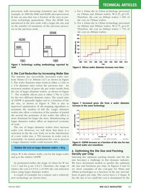
processors with increasing transistors per chip 6. For<br />
example, in 1989 the 8086 and 80286 microprocessors<br />
fit into an area that was a fraction <strong>of</strong> the area in previous<br />
technology generations. <strong>The</strong>n the 80486 was<br />
introduced in the new node with a larger die size and<br />
4x the number <strong>of</strong> transistors <strong>of</strong> the previous processor<br />
in the previous node.<br />
Figure 5 Technology scaling methodology reported by<br />
Intel<br />
5. Die Cost Reduction by Increasing Wafer Size<br />
<strong>The</strong> industry has successfully increased wafer size 7<br />
from 50mm (2”) to 300mm (12”) as shown in Figure<br />
6. <strong>The</strong> wafer diameter steps result in either a 1.33x or<br />
a 1.5x diameter ratio versus the previous size. An<br />
increased number <strong>of</strong> gross die per wafer results from<br />
the use <strong>of</strong> larger diameter wafers, as shown in Figure<br />
7. <strong>The</strong> available silicon area is either 1.78x or 2.25x<br />
for the two different diameter ratios. <strong>The</strong> actual ratio<br />
<strong>of</strong> GDPW is generally higher and is a function <strong>of</strong> the<br />
die size, as shown in Figure 8. This is due to<br />
improved optimization <strong>of</strong> die-stepping algorithms to<br />
maximize the number <strong>of</strong> full die. Larger diameter<br />
wafers also allow a reduction <strong>of</strong> the number <strong>of</strong> partial<br />
die around the perimeter <strong>of</strong> the wafer; this effect is<br />
more dominant for larger die sizes. Manufacturing on<br />
larger diameter wafers <strong>of</strong>fers an improved economy<br />
<strong>of</strong> scale.<br />
<strong>The</strong> use <strong>of</strong> larger diameter wafers does increase<br />
wafer cost. However, we will show that there is a<br />
reduction in the die cost. Early on in the introduction<br />
<strong>of</strong> a new wafer size, a 70% increase in wafer cost is<br />
reasonable 4. In mature production the cost to process<br />
a larger diameter wafer could increase 30%.<br />
Relative Die Cost on larger diameter wafers = W/g,<br />
where W is the relative wafer cost for the larger wafer<br />
and g is the relative GDPW<br />
As mentioned earlier, the range <strong>of</strong> values for W are<br />
1.3-1.7 and for g are 1.8-2.5. <strong>The</strong>refore, the range <strong>of</strong><br />
relative die cost is 0.5-0.9, a 10-50% die cost reduction<br />
when using larger diameter wafers.<br />
A couple <strong>of</strong> examples for a mature and a relatively<br />
new technology are shown here:<br />
TECHNICAL ARTICLES<br />
a. For a 10mm die in 0.8um technology processed<br />
on 150mm and 200mm wafers, W=1.35, g=1.95.<br />
<strong>The</strong>refore, die cost on 200mm wafers = 69% <strong>of</strong><br />
die cost on 150mm wafers.<br />
b. For a 10mm die in 130nm technology processed<br />
on 200mm and 300mm wafers, W=1.75, g=2.45.<br />
<strong>The</strong>refore, die cost on 300mm wafers = 71% <strong>of</strong><br />
die cost on 200mm wafers.<br />
Figure 6 Silicon wafer diameter increase over time<br />
Figure 7 Increased gross die from a wafer diameter<br />
increase in the same technology<br />
Figure 8 GDPW increase as a function <strong>of</strong> die size for two<br />
different wafer size transitions<br />
6. Optimizing the Die Size and Packing<br />
Density per Chip<br />
Selecting the optimum packing density and the die<br />
size becomes a challenge in this dynamic industry.<br />
We have developed models to predict the optimum<br />
die size and functions per chip. In Figures 9 and 10<br />
we show examples <strong>of</strong> the cost/gate for 90nm and<br />
180nm technologies as a function <strong>of</strong> die size and millions<br />
<strong>of</strong> gates per chip. <strong>The</strong> curves have a U-shape. If<br />
the die size is too small the cost is dominated by the<br />
Winter 2007 <strong>IEEE</strong> SSCS NEWSLETTER 25

