

The Impact of Dennard's Scaling Theory - IEEE
The Impact of Dennard's Scaling Theory - IEEE
The Impact of Dennard's Scaling Theory - IEEE
- TAGS
- scaling
- www.ieee.org

You also want an ePaper? Increase the reach of your titles
YUMPU automatically turns print PDFs into web optimized ePapers that Google loves.
A 30 Year Retrospective on Dennard’s MOSFET<br />
<strong>Scaling</strong> Paper<br />
Mark Bohr, Intel Corporation, mark.bohr@intel.com<br />
More than three decades have passed since the<br />
team <strong>of</strong> Robert Dennard, Fritz Gaensslen,<br />
Hwa-Nien Yu, V. Leo Rideout, Ernest Bassous<br />
and Andre LeBlanc from the IBM T. J. Watson Research<br />
Center wrote the seminal paper describing MOSFET<br />
scaling rules for obtaining simultaneous improvements<br />
in transistor density, switching speed and power dissipation<br />
[1]. At the time <strong>of</strong> this paper (1974), commercially<br />
available circuits were using MOSFETs with gate<br />
lengths <strong>of</strong> approximately 5 microns, but devices with<br />
shorter gate lengths were already being built in laboratories<br />
that were demonstrating the benefits <strong>of</strong> further<br />
scaling. <strong>The</strong> scaling principles described by Dennard<br />
and his team were quickly adopted by the semiconductor<br />
industry as the roadmap for providing systematic<br />
and predictable transistor improvements.<br />
Table I is reproduced from Dennard’s paper and<br />
summarizes transistor or circuit parameter changes<br />
under ideal scaling conditions, where κ is the unitless<br />
scaling constant. <strong>The</strong> tantalizing benefits <strong>of</strong> MOSFET<br />
device scaling immediately leap out from this table: as<br />
transistors get smaller, they can switch faster and use<br />
less power. But <strong>of</strong> course learning exactly how to<br />
make transistors smaller in a way that could be done<br />
practically in high volume manufacturing would take<br />
time. It would take time to develop lithographic techniques<br />
to pattern smaller feature sizes, to grow thinner<br />
gate oxides, and to reduce defect levels at these<br />
increasingly challenging dimensions. But this paper<br />
gave our industry a roadmap, a method for setting targets<br />
and expectations for coming generations <strong>of</strong><br />
process technology. This paper gave us the more specific<br />
transistor scaling formula needed to continue<br />
Moore’s Law, which was first articulated in a paper by<br />
Table I: <strong>Scaling</strong> Results for Circuit Performance (from Dennard)<br />
TECHNICAL ARTICLES<br />
Gordon Moore in 1965 and was in effect being followed<br />
by the semiconductor industry since the early<br />
1960’s. (To read reprints <strong>of</strong> Gordon Moore’s 1965 and<br />
1975 papers along with recent commentaries on<br />
Moore’s Law, see the September 2006 issue <strong>of</strong> the<br />
<strong>IEEE</strong> Solid-State Circuits Society Newsletter.)<br />
<strong>The</strong> ideas described in Moore’s and Dennard’s<br />
papers set our industry on a course <strong>of</strong> developing new<br />
integrated circuit process technologies and products on<br />
a regular pace and providing consistent improvements<br />
in transistor density, performance and power. Each new<br />
generation <strong>of</strong> process technology was expected to<br />
reduce minimum feature size by approximately 0.7x (κ<br />
~1.4). A 0.7x reduction in linear features size was generally<br />
considered to be a worthwhile step to take for a<br />
new process generation as it provided roughly a 2x<br />
increase in transistor density. During the 1970’s and<br />
1980’s the semiconductor industry was introducing new<br />
technology generations approximately every 3 years.<br />
This translates to transistor density improvements <strong>of</strong> ~2x<br />
every 3 years, but this was also a period when average<br />
chip sizes were increasing, resulting in transistor count<br />
increases <strong>of</strong> close to 4x every 3 years (or 2x every 18<br />
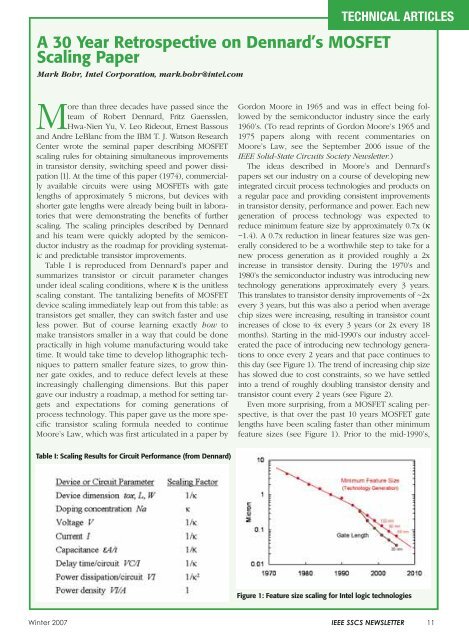
months). Starting in the mid-1990’s our industry accelerated<br />
the pace <strong>of</strong> introducing new technology generations<br />
to once every 2 years and that pace continues to<br />
this day (see Figure 1). <strong>The</strong> trend <strong>of</strong> increasing chip size<br />
has slowed due to cost constraints, so we have settled<br />
into a trend <strong>of</strong> roughly doubling transistor density and<br />
transistor count every 2 years (see Figure 2).<br />
Even more surprising, from a MOSFET scaling perspective,<br />
is that over the past 10 years MOSFET gate<br />
lengths have been scaling faster than other minimum<br />
feature sizes (see Figure 1). Prior to the mid-1990’s,<br />
Figure 1: Feature size scaling for Intel logic technologies<br />
Winter 2007 <strong>IEEE</strong> SSCS NEWSLETTER 11

