

The Impact of Dennard's Scaling Theory - IEEE
The Impact of Dennard's Scaling Theory - IEEE
The Impact of Dennard's Scaling Theory - IEEE
- TAGS
- scaling
- www.ieee.org

You also want an ePaper? Increase the reach of your titles
YUMPU automatically turns print PDFs into web optimized ePapers that Google loves.
TECHNICAL ARTICLES<br />
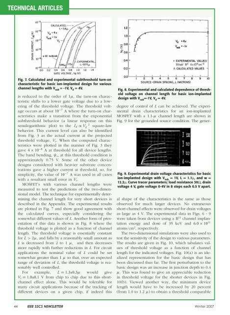
Fig. 7. Calculated and experimental subthreshold turn-on<br />
characteristic for basic ion-implanted design for various<br />
channel lengths with V sub = -1V, V d = 4V.<br />
is reduced to the order <strong>of</strong> 1μ, the turn-on characteristic<br />
shifts to a lower gate voltage due to a lowering<br />
<strong>of</strong> the threshold voltage. <strong>The</strong> threshold voltage<br />
occurs at about 10 −7 A where the turn-on characteristics<br />
make a transition from the exponential<br />
subthreshold behavior (a linear response on this<br />
semilogarithmic plot) to the Id ∝ Vg 2 square-law<br />
behavior. This current level can also be identified<br />
from Fig. 3 as the actual current at the projected<br />
threshold voltage, Vt . When the computed characteristics<br />
were plotted in the manner <strong>of</strong> Fig. 3 they<br />
gave 4 × 10 −8 A at threshold for all device lengths.<br />
<strong>The</strong> band bending, ψs, at this threshold condition is<br />
approximately 0.75 V. Some <strong>of</strong> the other device<br />
designs considered with heavier substrate concentrations<br />
gave a higher current at threshold, so, for<br />
simplicity, the value <strong>of</strong> 10 −7 A was used in all cases<br />
with a resultant small error in Vt .<br />
MOSFET’s with various channel lengths were<br />
measured to test the predictions <strong>of</strong> the two-dimensional<br />
model. <strong>The</strong> technique for experimentally determining<br />
the channel length for very short devices is<br />
described in the Appendix. <strong>The</strong> experimental results<br />
are plotted in Fig. 7 and show good agreement with<br />
the calculated curves, especially considering the<br />
somewhat different values <strong>of</strong> L. Another form <strong>of</strong> presentation<br />
<strong>of</strong> this data is shown in Fig. 8 where the<br />
threshold voltage is plotted as a function <strong>of</strong> channel<br />
length. <strong>The</strong> threshold voltage is essentially constant<br />
for L > 2μ, and falls by a reasonably small amount as<br />
L is decreased from 2 to 1 μ, and then decreases<br />
more rapidly with further reductions in L. For circuit<br />
applications the nominal value <strong>of</strong> L could be set<br />
somewhat greater than 1 μ so that, over an expected<br />
range <strong>of</strong> deviation <strong>of</strong> L, the threshold voltage is reasonably<br />
well controlled.<br />
For example, L = 1.3±0.3μ would give<br />
Vt = 1.0±0.1 V from chip to chip due to this shortchannel<br />
effect alone. This would be tolerable for<br />
many circuit applications because <strong>of</strong> the tracking <strong>of</strong><br />
different devices on a given chip, if indeed this<br />
Fig. 8. Experimental and calculated dependence <strong>of</strong> threshold<br />
voltage on channel length for basic ion-implanted<br />
design with V sub =-1V, V d = 4V.<br />
degree <strong>of</strong> control <strong>of</strong> L can be achieved. <strong>The</strong> experimental<br />
drain characteristics for an ion-implanted<br />
MOSFET with a 1.1-μ channel length are shown in<br />
Fig. 9 for the grounded source condition. <strong>The</strong> gener-<br />
Fig. 9. Experimental drain voltage characteristics for basic<br />
ion-implanted design with V sub = 1V, L = 1.1μ, and w =<br />
12.2μ. Curve tracer parameters; load resistance 30Ω, drain<br />
voltage 4 V, gate voltage 0-4V in 8 steps each 0.5 V apart.<br />
al shape <strong>of</strong> the characteristics is the same as those<br />
observed for much larger devices. No extraneous<br />
short-channel effects were observed for drain voltages<br />
as large as 4 V. <strong>The</strong> experimental data in Figs. 6 - 9<br />
were taken from devices using a B 11 channel implantation<br />
energy and dose <strong>of</strong> 35 keV and 6.0 × 10 11<br />
atoms/cm 2 , respectively.<br />
<strong>The</strong> two-dimensional simulations were also used to<br />
test the sensitivity <strong>of</strong> the design to various parameters.<br />
<strong>The</strong> results are given in Fig. 10, which tabulates values<br />
<strong>of</strong> threshold voltage as a function <strong>of</strong> channel<br />
length for the indicated voltages. Fig. 10(a) is an idealized<br />
representation for the basic design that has<br />
been discussed thus far. <strong>The</strong> first perturbation to the<br />
basic design was an increase in junction depth to 0.4<br />
μ. This was found to give an appreciable reduction<br />
in threshold voltage for the shorter devices in Fig.<br />
10(b). Viewed another way, the minimum device<br />
length would have to be increased by 20 percent<br />
(from 1.0 to 1.2 μ) to obtain a threshold comparable<br />
44 <strong>IEEE</strong> SSCS NEWSLETTER Winter 2007

