

The Impact of Dennard's Scaling Theory - IEEE
The Impact of Dennard's Scaling Theory - IEEE
The Impact of Dennard's Scaling Theory - IEEE
- TAGS
- scaling
- www.ieee.org

Create successful ePaper yourself
Turn your PDF publications into a flip-book with our unique Google optimized e-Paper software.
TECHNICAL ARTICLES<br />
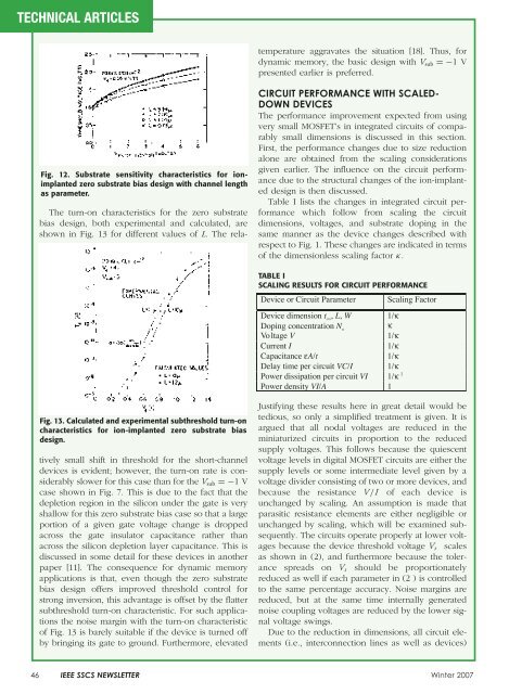
Fig. 12. Substrate sensitivity characteristics for ionimplanted<br />
zero substrate bias design with channel length<br />
as parameter.<br />
<strong>The</strong> turn-on characteristics for the zero substrate<br />
bias design, both experimental and calculated, are<br />
shown in Fig. 13 for different values <strong>of</strong> L. <strong>The</strong> rela-<br />
Fig. 13. Calculated and experimental subthreshold turn-on<br />
characteristics for ion-implanted zero substrate bias<br />
design.<br />
tively small shift in threshold for the short-channel<br />
devices is evident; however, the turn-on rate is considerably<br />
slower for this case than for the Vsub =−1 V<br />
case shown in Fig. 7. This is due to the fact that the<br />
depletion region in the silicon under the gate is very<br />
shallow for this zero substrate bias case so that a large<br />
portion <strong>of</strong> a given gate voltage change is dropped<br />
across the gate insulator capacitance rather than<br />
across the silicon depletion layer capacitance. This is<br />
discussed in some detail for these devices in another<br />
paper [11]. <strong>The</strong> consequence for dynamic memory<br />
applications is that, even though the zero substrate<br />
bias design <strong>of</strong>fers improved threshold control for<br />
strong inversion, this advantage is <strong>of</strong>fset by the flatter<br />
subthreshold turn-on characteristic. For such applications<br />
the noise margin with the turn-on characteristic<br />
<strong>of</strong> Fig. 13 is barely suitable if the device is turned <strong>of</strong>f<br />
by bringing its gate to ground. Furthermore, elevated<br />
temperature aggravates the situation [18]. Thus, for<br />
dynamic memory, the basic design with Vsub =−1 V<br />
presented earlier is preferred.<br />
CIRCUIT PERFORMANCE WITH SCALED-<br />
DOWN DEVICES<br />
<strong>The</strong> performance improvement expected from using<br />
very small MOSFET’s in integrated circuits <strong>of</strong> comparably<br />
small dimensions is discussed in this section.<br />
First, the performance changes due to size reduction<br />
alone are obtained from the scaling considerations<br />
given earlier. <strong>The</strong> influence on the circuit performance<br />
due to the structural changes <strong>of</strong> the ion-implanted<br />
design is then discussed.<br />
Table I lists the changes in integrated circuit performance<br />
which follow from scaling the circuit<br />
dimensions, voltages, and substrate doping in the<br />
same manner as the device changes described with<br />
respect to Fig. 1. <strong>The</strong>se changes are indicated in terms<br />
<strong>of</strong> the dimensionless scaling factor κ.<br />
TABLE I<br />
SCALING RESULTS FOR CIRCUIT PERFORMANCE<br />
Justifying these results here in great detail would be<br />
tedious, so only a simplified treatment is given. It is<br />
argued that all nodal voltages are reduced in the<br />
miniaturized circuits in proportion to the reduced<br />
supply voltages. This follows because the quiescent<br />
voltage levels in digital MOSFET circuits are either the<br />
supply levels or some intermediate level given by a<br />
voltage divider consisting <strong>of</strong> two or more devices, and<br />
because the resistance V /I <strong>of</strong> each device is<br />
unchanged by scaling. An assumption is made that<br />
parasitic resistance elements are either negligible or<br />
unchanged by scaling, which will be examined subsequently.<br />
<strong>The</strong> circuits operate properly at lower voltages<br />
because the device threshold voltage Vt scales<br />
as shown in (2), and furthermore because the tolerance<br />
spreads on Vt should be proportionately<br />
reduced as well if each parameter in (2 ) is controlled<br />
to the same percentage accuracy. Noise margins are<br />
reduced, but at the same time internally generated<br />
noise coupling voltages are reduced by the lower signal<br />
voltage swings.<br />
Due to the reduction in dimensions, all circuit elements<br />
(i.e., interconnection lines as well as devices)<br />
46 <strong>IEEE</strong> SSCS NEWSLETTER Winter 2007

