

The Impact of Dennard's Scaling Theory - IEEE
The Impact of Dennard's Scaling Theory - IEEE
The Impact of Dennard's Scaling Theory - IEEE
- TAGS
- scaling
- www.ieee.org

Create successful ePaper yourself
Turn your PDF publications into a flip-book with our unique Google optimized e-Paper software.
Analog IC Design at the University <strong>of</strong> Twente<br />
Bram Nauta, IC Design Group, University <strong>of</strong> Twente, Enschede, <strong>The</strong> Netherlands,<br />
b.nauta@utwente.nl<br />
Introduction<br />
This article describes some recent research results<br />
from the IC Design group <strong>of</strong> the University <strong>of</strong> Twente,<br />
located in Enschede, <strong>The</strong> Netherlands.<br />
Our research focuses on analog CMOS circuit<br />
design with emphasis on high frequency and broadband<br />
circuits. With the trend <strong>of</strong> system integration in<br />
mind, we try to develop new circuit techniques that<br />
enable the next steps in system integration in<br />
nanometer CMOS technology. Our research funding<br />
comes from industry, as well as from governmental<br />
organizations. We aim to find fundamental solutions<br />
for practical problems <strong>of</strong> integrated circuits realized in<br />
industrial Silicon technologies.<br />
CMOS IC technology is dictated by optimal cost and<br />
performance <strong>of</strong> digital circuits and is certainly not<br />
optimized for nice analog behavior. As analog designers,<br />
we do not have the illusion <strong>of</strong> being able to<br />
change CMOS technology, so we have to “live with it”<br />
and solve the problems by design. In this article several<br />
examples will be shown where problematic analog<br />
behavior, such as noise and distortion, can be tackled<br />
with new circuit design techniques. <strong>The</strong>se circuit<br />
techniques are developed in such a way that they do<br />
benefit from modern technology and thus enable further<br />
integration. This way we can improve various<br />
analog building blocks for wireless, wire-line and optical<br />
communication. Below some examples are given.<br />
<strong>The</strong>rmal Noise Cancelling<br />
Noise is an important issue; in communication circuits<br />
the sensitivity <strong>of</strong> the receiver is limited by the noise<br />
level <strong>of</strong> the circuits. Especially, the noise <strong>of</strong> the first<br />
amplifier in the receiving chain is <strong>of</strong> high importance,<br />
since after that amplifier the signal is stronger and the<br />
allowable noise levels are higher. For narrowband<br />
receivers the added noise <strong>of</strong> the amplifier can be<br />
reduced relatively easily. This is done by using resonant<br />
structures, built with - for example - integrated<br />
spiral inductors and capacitors which provide voltage<br />
gain <strong>of</strong> the narrowband signals and therefore needing<br />
less gain from “noisy” transistors. For wideband systems,<br />
e.g. for TV tuners, UWB (Ultra Wide Band)<br />
communication and future s<strong>of</strong>tware defined radio,<br />
several octaves <strong>of</strong> bandwidth are needed and simple<br />
resonant structures cannot be used. For these applications,<br />
low noise gain stages using noisy transistors<br />
have to be used, which is quite a challenge. Apart<br />
from the gain and noise demands, additional<br />
demands, such as input impedance matching and<br />
good linearity, need to be satisfied.<br />
RESEARCH HIGHLIGHTS<br />
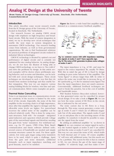
Figure 1a shows a wide band first amplifier stage,<br />
denoted as a common-source feedback amplifier.<br />
Fig 1a: common source LNA with impedance matching,<br />
the signals at nodes X and Y have opposite sign.<br />
Fig 1b: <strong>The</strong> noise <strong>of</strong> M1 generates in-phase noise voltages<br />
at nodes X and Y.<br />
<strong>The</strong> input impedance is 1/g m <strong>of</strong> M1, and must be<br />
equal to the source impedance Rs, usually 50 Ohms.<br />
With this in mind the gm <strong>of</strong> M1 is fixed by design<br />
resulting in poor noise behavior <strong>of</strong> the amplifier: <strong>The</strong><br />
"noise figure" is always larger than 3dB. In order to<br />
reduce the noise one would like to increase the g m <strong>of</strong><br />
M1 (preferably g m>>1/Rs for minimal noise figure) but<br />
then the input impedance does not match anymore.<br />
Conventionally, additional feedback techniques are<br />
used to break this paradox, but at the cost <strong>of</strong> stability<br />
and bandwidth issues.<br />
PhD Student Federico Bruccoleri realized, however,<br />
that generated noise can be cancelled by proper<br />
circuit design. If we take a look at Figure 1b, we can<br />
see how the noise current <strong>of</strong> M1 flows in the circuit;<br />
this is indicated by the red arrow.<br />
<strong>The</strong> noise current due to M1 flows in a loop,<br />
through Rs. This noise current generates a noise voltage<br />
at nodes X and Y which are <strong>of</strong> different magnitude<br />
but <strong>of</strong> the same phase. <strong>The</strong> signals nodes X and<br />
Y are in anti-phase due to the inverting nature <strong>of</strong> this<br />
amplifier. So somehow it should be possible to separate<br />
the signal from the noise!<br />
By adding an additional amplifier “A,” as shown in<br />
Figure 2, we can construct an output signal in such a<br />
way the wanted signals at nodes X and Y are added<br />
and that the noise at nodes X and Y are cancelled [1].<br />
This way we can cancel the noise <strong>of</strong> M1, which holds<br />
for both thermal and 1/f noise. Of course amplifier<br />
“A” will now add additional noise, but this needs not<br />
to be a problem. <strong>The</strong> reason for this is that in contrast<br />
to M1, we can choose the gm <strong>of</strong> the input stage <strong>of</strong><br />
amplifier “A” relatively large, and thus make it low-<br />
Winter 2007 <strong>IEEE</strong> SSCS NEWSLETTER 5

