

The Impact of Dennard's Scaling Theory - IEEE
The Impact of Dennard's Scaling Theory - IEEE
The Impact of Dennard's Scaling Theory - IEEE
- TAGS
- scaling
- www.ieee.org

You also want an ePaper? Increase the reach of your titles
YUMPU automatically turns print PDFs into web optimized ePapers that Google loves.
improvements in process control, cycle-time, and overall<br />
flexibility and continue the scaling <strong>of</strong> devices to deep<br />
submicron to cost effectively. In particular, the MMST<br />
Program demonstrated the technical feasibility <strong>of</strong> 100%<br />
single-wafer processing, dynamic/object-oriented Computer-Integrated-Manufacturing<br />
(CIM), real-time/modelbased<br />
process control, in-situ sensors, 95% dry processing,<br />
and integrated mini environments.<br />
At that time, state-<strong>of</strong>-the-art commercial wafer fabs<br />
used a mix <strong>of</strong> approximately 60% single-wafer and<br />
40% batch processing equipment. Since then, complete<br />
sets <strong>of</strong> commercial single-wafer process tools<br />
have become available and are the norm for deep<br />
submicron manufacturing.<br />
<strong>The</strong> most significant contribution <strong>of</strong> MMST to single-wafer<br />
processing was in the area <strong>of</strong> Rapid <strong>The</strong>rmal<br />
Processing (RTP). In contrast to large furnaces for<br />
thermal processing, the MMST program developed<br />
processing chambers in which single wafers were<br />
heated by lamps under multi-zone, closed-loop wafer-<br />
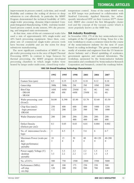
1992 SIA Overall Roadmap Technology Characteristics<br />
TECHNICAL ARTICLES<br />
temperature control. Some <strong>of</strong> the initial MMST work<br />
on RTP lamps was performed in collaboration with<br />
Stanford University. Applied Materials, Inc. subsequently<br />
introduced RTP on their Centura HT cluster<br />
tool. MMST also created the first lithography cluster<br />
tool and the concept <strong>of</strong> the vacuum carrier which is<br />
more popularly knows as the SMIF box.<br />
SIA Industry Roadmap<br />
In November 1992, 179 <strong>of</strong> the key semiconductor technologists<br />
<strong>of</strong> the US gathered in Irving, Texas for a historic<br />
workshop to create a common vision for the course<br />
<strong>of</strong> the semiconductor industry for the next 15 years<br />
based on scaling technology 8. <strong>The</strong> group consisted primarily<br />
<strong>of</strong> scientists and engineers from the US Semiconductor<br />
Industry and a liberal sprinkling <strong>of</strong> academics,<br />
government agencies and national laboratories. <strong>The</strong><br />
workshop, sponsored by the Semiconductor Industry<br />
Association and coordinated by Semiconductor Research<br />
Corporation and Sematech, created the roadmap below.<br />
Winter 2007 <strong>IEEE</strong> SSCS NEWSLETTER 15

