

The Impact of Dennard's Scaling Theory - IEEE
The Impact of Dennard's Scaling Theory - IEEE
The Impact of Dennard's Scaling Theory - IEEE
- TAGS
- scaling
- www.ieee.org

You also want an ePaper? Increase the reach of your titles
YUMPU automatically turns print PDFs into web optimized ePapers that Google loves.
TECHNICAL ARTICLES<br />
Figure 2: Transistor count trend for Intel microprocessors<br />
gate lengths were roughly the same size as other minimum<br />
process features, but starting with the 0.35 μm<br />
generation, gate lengths have been scaling faster than<br />
0.7x per generation to realize performance advantages,<br />
even though gate pitch has been scaling at the<br />
normal rate. This has been a key factor in microprocessors<br />
achieving >3 GHz operating frequencies<br />
sooner than most experts thought possible even 10<br />
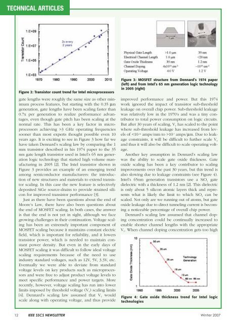
years ago. It is exciting to see in Figure 3 how far we<br />
have taken Dennard’s scaling law by comparing the 1<br />
mm transistor described in his 1974 paper to the 35<br />
nm gate length transistor used in Intel’s 65 nm generation<br />
logic technology that started high volume manufacturing<br />
in 2005 [2]. <strong>The</strong> Intel transistor shown in<br />
Figure 3 provides an example <strong>of</strong> an emerging trend<br />
among semiconductor manufacturers: the introduction<br />
<strong>of</strong> new structures and materials to extend transistor<br />
scaling. In this case the new feature is selectively<br />
deposited SiGe source-drains to provide strained silicon<br />
for improved transistor performance [3].<br />
Just as there have been questions about the end <strong>of</strong><br />
Moore’s Law, there have also been questions about<br />
the end <strong>of</strong> MOSFET scaling. In both cases, the answer<br />
is that the end is not yet in sight, although we face<br />
growing challenges in their continuation. Voltage scaling<br />
has been an extremely important component <strong>of</strong><br />
MOSFET scaling because it maintains constant electric<br />
field, which is important for reliability, and it lowers<br />
transistor power, which is needed to maintain constant<br />
power density. But even in the early days <strong>of</strong><br />
MOSFET scaling it was difficult to follow ideal voltage<br />
scaling requirements because <strong>of</strong> the need to use<br />
industry standard voltages, such as 12V, 5V, 3.3V, etc.<br />
Eventually we were able to deviate from standard<br />
voltage levels on key products such as microprocessors<br />
and were free to adjust product voltage levels to<br />
meet specific performance and power targets. More<br />
recently, however, voltage scaling has run into lower<br />
limits imposed by threshold voltage (V T) scaling limits<br />
[4]. Dennard’s scaling law assumed that V T would<br />
scale along with operating voltage, and thus provide<br />
Figure 3: MOSFET structure from Dennard’s 1974 paper<br />
(left) and from Intel’s 65 nm generation logic technology<br />
in 2005 (right)<br />
improved performance and power. But this 1974<br />
work ignored the impact <strong>of</strong> transistor sub-threshold<br />
leakage on overall chip power. Sub-threshold leakage<br />
was relatively low in the 1970’s and was a tiny contributor<br />
to total power consumption on logic circuits.<br />
But after 30 years <strong>of</strong> scaling, V T has scaled to the point<br />
where sub-threshold leakage has increased from levels<br />
<strong>of</strong> 10 -7 amps/μm. Due to leakage<br />
constraints, it will be difficult to further scale V T<br />
and thus it will also be difficult to scale operating voltage.<br />
Another key assumption in Dennard’s scaling law<br />
was the ability to scale gate oxide thickness. Gate<br />
oxide scaling has been a key contributor to scaling<br />
improvements over the past 30 years, but this trend is<br />
also slowing due to leakage constraints (see Figure 4).<br />
Intel’s 65nm generation transistors use a SiO 2 gate<br />
dielectric with a thickness <strong>of</strong> 1.2 nm [2]. This dielectric<br />
is only about 5 silicon atomic layers thick and represents<br />
what is likely the limit to which SiO 2 can be<br />
scaled. Not only are we running out <strong>of</strong> atoms, but gate<br />
oxide leakage due to direct tunneling current is becoming<br />
a noticeable percentage <strong>of</strong> overall chip power.<br />
Dennard’s scaling law assumed that channel doping<br />
concentration could be continually increased to<br />
enable shorter channel lengths with the appropriate<br />
V T. When channel doping concentration gets too high<br />
Figure 4: Gate oxide thickness trend for Intel logic<br />
technologies<br />
12 <strong>IEEE</strong> SSCS NEWSLETTER Winter 2007

