

The Impact of Dennard's Scaling Theory - IEEE
The Impact of Dennard's Scaling Theory - IEEE
The Impact of Dennard's Scaling Theory - IEEE
- TAGS
- scaling
- www.ieee.org

Create successful ePaper yourself
Turn your PDF publications into a flip-book with our unique Google optimized e-Paper software.
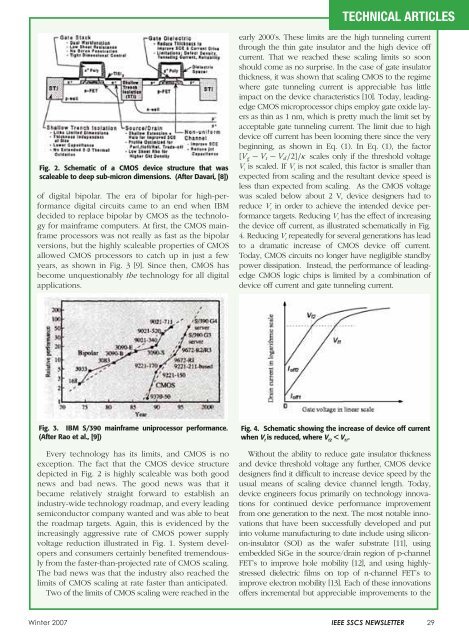
Fig. 2. Schematic <strong>of</strong> a CMOS device structure that was<br />
scaleable to deep sub-micron dimensions. (After Davari, [8])<br />
<strong>of</strong> digital bipolar. <strong>The</strong> era <strong>of</strong> bipolar for high-performance<br />
digital circuits came to an end when IBM<br />
decided to replace bipolar by CMOS as the technology<br />
for mainframe computers. At first, the CMOS mainframe<br />
processors was not really as fast as the bipolar<br />
versions, but the highly scaleable properties <strong>of</strong> CMOS<br />
allowed CMOS processors to catch up in just a few<br />
years, as shown in Fig. 3 [9]. Since then, CMOS has<br />
become unquestionably the technology for all digital<br />
applications.<br />
Fig. 3. IBM S/390 mainframe uniprocessor performance.<br />
(After Rao et al., [9])<br />
Every technology has its limits, and CMOS is no<br />
exception. <strong>The</strong> fact that the CMOS device structure<br />
depicted in Fig. 2 is highly scaleable was both good<br />
news and bad news. <strong>The</strong> good news was that it<br />
became relatively straight forward to establish an<br />
industry-wide technology roadmap, and every leading<br />
semiconductor company wanted and was able to beat<br />
the roadmap targets. Again, this is evidenced by the<br />
increasingly aggressive rate <strong>of</strong> CMOS power supply<br />
voltage reduction illustrated in Fig. 1. System developers<br />
and consumers certainly benefited tremendously<br />
from the faster-than-projected rate <strong>of</strong> CMOS scaling.<br />
<strong>The</strong> bad news was that the industry also reached the<br />
limits <strong>of</strong> CMOS scaling at rate faster than anticipated.<br />
Two <strong>of</strong> the limits <strong>of</strong> CMOS scaling were reached in the<br />
TECHNICAL ARTICLES<br />
early 2000’s. <strong>The</strong>se limits are the high tunneling current<br />
through the thin gate insulator and the high device <strong>of</strong>f<br />
current. That we reached these scaling limits so soon<br />
should come as no surprise. In the case <strong>of</strong> gate insulator<br />
thickness, it was shown that scaling CMOS to the regime<br />
where gate tunneling current is appreciable has little<br />
impact on the device characteristics [10]. Today, leadingedge<br />
CMOS microprocessor chips employ gate oxide layers<br />
as thin as 1 nm, which is pretty much the limit set by<br />
acceptable gate tunneling current. <strong>The</strong> limit due to high<br />
device <strong>of</strong>f current has been looming there since the very<br />
beginning, as shown in Eq. (1). In Eq. (1), the factor<br />
[Vg − Vt − Vd /2]/κ scales only if the threshold voltage<br />
V t is scaled. If V t is not scaled, this factor is smaller than<br />
expected from scaling and the resultant device speed is<br />
less than expected from scaling. As the CMOS voltage<br />
was scaled below about 2 V, device designers had to<br />
reduce V t in order to achieve the intended device performance<br />
targets. Reducing V t has the effect <strong>of</strong> increasing<br />
the device <strong>of</strong>f current, as illustrated schematically in Fig.<br />
4. Reducing V t repeatedly for several generations has lead<br />
to a dramatic increase <strong>of</strong> CMOS device <strong>of</strong>f current.<br />
Today, CMOS circuits no longer have negligible standby<br />
power dissipation. Instead, the performance <strong>of</strong> leadingedge<br />
CMOS logic chips is limited by a combination <strong>of</strong><br />
device <strong>of</strong>f current and gate tunneling current.<br />
Fig. 4. Schematic showing the increase <strong>of</strong> device <strong>of</strong>f current<br />
when V t is reduced, where V t2 < V t1 .<br />
Without the ability to reduce gate insulator thickness<br />
and device threshold voltage any further, CMOS device<br />
designers find it difficult to increase device speed by the<br />
usual means <strong>of</strong> scaling device channel length. Today,<br />
device engineers focus primarily on technology innovations<br />
for continued device performance improvement<br />
from one generation to the next. <strong>The</strong> most notable innovations<br />
that have been successfully developed and put<br />
into volume manufacturing to date include using siliconon-insulator<br />
(SOI) as the wafer substrate [11], using<br />
embedded SiGe in the source/drain region <strong>of</strong> p-channel<br />
FET’s to improve hole mobility [12], and using highlystressed<br />
dielectric films on top <strong>of</strong> n-channel FET’s to<br />
improve electron mobility [13]. Each <strong>of</strong> these innovations<br />
<strong>of</strong>fers incremental but appreciable improvements to the<br />
Winter 2007 <strong>IEEE</strong> SSCS NEWSLETTER 29

