

The Impact of Dennard's Scaling Theory - IEEE
The Impact of Dennard's Scaling Theory - IEEE
The Impact of Dennard's Scaling Theory - IEEE
- TAGS
- scaling
- www.ieee.org

You also want an ePaper? Increase the reach of your titles
YUMPU automatically turns print PDFs into web optimized ePapers that Google loves.
10. References<br />
1. G.E. Moore, “Progress in Digital Electronics”,<br />
1975 IEDM, pp11-13.<br />
2. G.E.Moore, “No Exponential is Forever; but “Forever”<br />
can be delayed”, ISSCC 2003, Paper 1.1.<br />
3. International Technology Roadmap for Semiconductors<br />
2005, http://public.itrs.net<br />
4. IC Knowledge, www.icknowledge.com<br />
5. W.Haensch, E.Nowak, R.H.Dennard, et. al., “Silicon<br />
CMOS Devices beyond scaling”, IBM J. Res.<br />
and Dev., Vol. 50, April/May 2006.<br />
6. P. Gelsinger, P. Gargini, G. Parker, A. Yu, “2001:<br />
A Microprocessor Odyssey”, published in “Technology<br />
2001”, MIT Press, pp. 95-113, July 1992.<br />
7. P. Gelsinger, “Moore’s Law – <strong>The</strong> Genius Lives<br />
On”, <strong>IEEE</strong> SSCS Newsletter, September 2006.<br />
8. R.C.Leachman, “Yield Modeling”, http://www.ieor.<br />
berkeley.edu/~ieor130/yield_models.pdf<br />
9. M.Sydow, “Compare Logic-Array To ASIC-Chip<br />
Cost per Good Die”, Chip Design Magazine, February/March<br />
2006.<br />
10. T.C. Chen, “Where CMOS is Going: Trendy Hype<br />
vs. Real Tecdhnology”, ISSCC 2006, Paper 1.1.<br />
TECHNICAL ARTICLES<br />
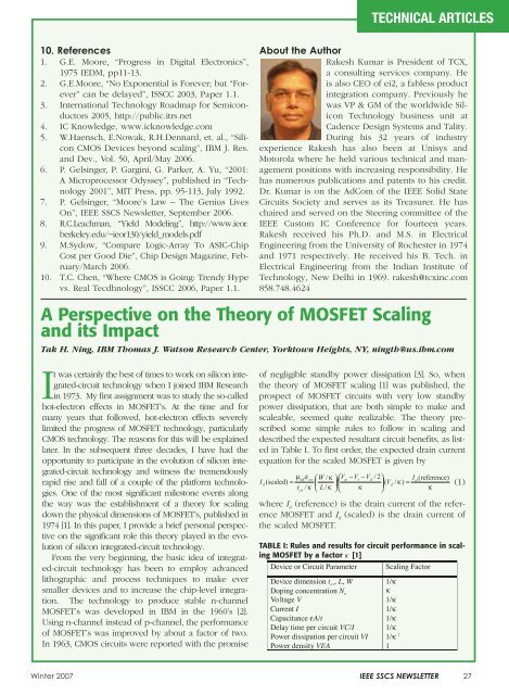
About the Author<br />
Rakesh Kumar is President <strong>of</strong> TCX,<br />
a consulting services company. He<br />
is also CEO <strong>of</strong> ei2, a fabless product<br />
integration company. Previously he<br />
was VP & GM <strong>of</strong> the worldwide Silicon<br />
Technology business unit at<br />
Cadence Design Systems and Tality.<br />
During his 32 years <strong>of</strong> industry<br />
experience Rakesh has also been at Unisys and<br />
Motorola where he held various technical and management<br />
positions with increasing responsibility. He<br />
has numerous publications and patents to his credit.<br />
Dr. Kumar is on the AdCom <strong>of</strong> the <strong>IEEE</strong> Solid State<br />
Circuits Society and serves as its Treasurer. He has<br />
chaired and served on the Steering committee <strong>of</strong> the<br />
<strong>IEEE</strong> Custom IC Conference for fourteen years.<br />
Rakesh received his Ph.D. and M.S. in Electrical<br />
Engineering from the University <strong>of</strong> Rochester in 1974<br />
and 1971 respectively. He received his B. Tech. in<br />
Electrical Engineering from the Indian Institute <strong>of</strong><br />
Technology, New Delhi in 1969. rakesh@tcxinc.com<br />
858.748.4624<br />
A Perspective on the <strong>The</strong>ory <strong>of</strong> MOSFET <strong>Scaling</strong><br />
and its <strong>Impact</strong><br />
Tak H. Ning, IBM Thomas J. Watson Research Center, Yorktown Heights, NY, ningth@us.ibm.com<br />
It was certainly the best <strong>of</strong> times to work on silicon integrated-circuit<br />
technology when I joined IBM Research<br />
in 1973. My first assignment was to study the so-called<br />
hot-electron effects in MOSFET’s. At the time and for<br />
many years that followed, hot-electron effects severely<br />
limited the progress <strong>of</strong> MOSFET technology, particularly<br />
CMOS technology. <strong>The</strong> reasons for this will be explained<br />
later. In the subsequent three decades, I have had the<br />
opportunity to participate in the evolution <strong>of</strong> silicon integrated-circuit<br />
technology and witness the tremendously<br />
rapid rise and fall <strong>of</strong> a couple <strong>of</strong> the platform technologies.<br />
One <strong>of</strong> the most significant milestone events along<br />
the way was the establishment <strong>of</strong> a theory for scaling<br />
down the physical dimensions <strong>of</strong> MOSFET’s, published in<br />
1974 [1]. In this paper, I provide a brief personal perspective<br />
on the significant role this theory played in the evolution<br />
<strong>of</strong> silicon integrated-circuit technology.<br />
From the very beginning, the basic idea <strong>of</strong> integrated-circuit<br />
technology has been to employ advanced<br />
lithographic and process techniques to make ever<br />
smaller devices and to increase the chip-level integration.<br />
<strong>The</strong> technology to produce stable n-channel<br />
MOSFET’s was developed in IBM in the 1960’s [2].<br />
Using n-channel instead <strong>of</strong> p-channel, the performance<br />
<strong>of</strong> MOSFET’s was improved by about a factor <strong>of</strong> two.<br />
In 1963, CMOS circuits were reported with the promise<br />
<strong>of</strong> negligible standby power dissipation [3]. So, when<br />
the theory <strong>of</strong> MOSFET scaling [1] was published, the<br />
prospect <strong>of</strong> MOSFET circuits with very low standby<br />
power dissipation, that are both simple to make and<br />
scaleable, seemed quite realizable. <strong>The</strong> theory prescribed<br />
some simple rules to follow in scaling and<br />
described the expected resultant circuit benefits, as listed<br />
in Table I. To first order, the expected drain current<br />
equation for the scaled MOSFET is given by<br />
Winter 2007 <strong>IEEE</strong> SSCS NEWSLETTER 27<br />
(1)<br />
where I d (reference) is the drain current <strong>of</strong> the reference<br />
MOSFET and I d (scaled) is the drain current <strong>of</strong><br />
the scaled MOSFET.<br />
TABLE I: Rules and results for circuit performance in scaling<br />
MOSFET by a factor κ [1]

