

The Impact of Dennard's Scaling Theory - IEEE
The Impact of Dennard's Scaling Theory - IEEE
The Impact of Dennard's Scaling Theory - IEEE
- TAGS
- scaling
- www.ieee.org

You also want an ePaper? Increase the reach of your titles
YUMPU automatically turns print PDFs into web optimized ePapers that Google loves.
Message from the President<br />
In 2007, look for an unadvertised bonus<br />
with your SSCS membership: A free<br />
subscription to the brand new quarterly<br />
Nanotechnology Magazine. We believe<br />
that circuit experts need to be in touch<br />
with this rapidly progressing technology.<br />
Some day it will be a fruitful area<br />
for circuits development, and opportunities to contribute<br />
will arise.<br />
<strong>The</strong> minimal subscription cost to the Society for the<br />
launch year <strong>of</strong> the new magazine prompted the AdCom<br />
to join the Nanotechnology Council. We hope the<br />
Council’s magazine effort will be <strong>of</strong> comparable interest<br />
to its Transactions on Nanotechnology, which is just<br />
beginning its sixth year and has among the highest rates<br />
<strong>of</strong> citation as measured by the Thompson ISI. I would<br />
like to receive feedback from you on how useful a tool<br />
the new magazine is. Look for the first issue in the<br />
spring <strong>of</strong> 2007.<br />
2007 is the Society’s 10th anniversary, having<br />
evolved from the Solid-State Circuits Council that originated<br />
in 1970. We’ve updated the SSCS logo for this<br />
year to draw attention to our progress. Since 1997, the<br />
Journal <strong>of</strong> Solid-State Circuits has increased coverage <strong>of</strong><br />
technical articles by 40%, and the SSCS Newsletter by 2<br />
1/2 times. <strong>The</strong> JSSC continues to be the most read in<br />
<strong>IEEE</strong> Xplore and the most cited in patents. Your SSCS<br />
membership provides online access not only to the<br />
Journal but also to the digests <strong>of</strong> our five major solidstate<br />
circuits conferences and most <strong>of</strong> their historic<br />
record. Local chapters have grown from 2 to 59, with<br />
Corrections<br />
In the article entitled “Overview <strong>of</strong><br />
CMOS Technology Development in<br />
the MIRAI Project,” by Toshiaki<br />
Masuhara and Masataka Hirose in<br />
the September 2006 issue, the last<br />
sentence in the Section entitled<br />
“New Circuits and System Technology<br />
- Post-fabrication Adaptive<br />
Adjustment” contains an incorrect<br />
expression, which is corrected as in<br />
the underlined expression in the following<br />
sentence:<br />
“As shown in Fig. 3, the developed<br />
tool successfully extracted the<br />
34 model parameters in 23 hours<br />
with a PC and resulted in a mean<br />
RMS error <strong>of</strong> 1.83% for benchmark<br />
MOSFETs.”<br />
In the Section, “New Gate Stack<br />
Technology with High-k Materials”,<br />
the caption for Figure 4 should read:<br />
Fig. 4 Gate leakage current in<br />
MIRAI HfAlON formed by Layer-by-<br />
Layer Deposition and Annealing<br />
(LL-D&A) 4 ).<br />
(a) Comparison <strong>of</strong> gate leakage current<br />
in MOSFETs with HfAlON<br />
gate insulator and HfSiON 5 ).<br />
(b) Cross sectional TEM micrograph<br />
<strong>of</strong> HfAlON/SiO 2 /Si gate stack<br />
formed by Layer-by-Layer Deposition<br />
and Annealing.<br />
<strong>The</strong> following corrections pertain<br />
to the reprint <strong>of</strong> “Lithography and<br />
the Future <strong>of</strong> Moore’s Law” (Moore,<br />
1995) in the September 2006 issue:<br />
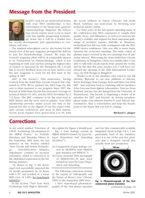
I have reproduced photomicrographs<br />
<strong>of</strong> the first planar transistor<br />
the recent addition <strong>of</strong> Tainan (Taiwan) and South<br />
Brazil. Celebrate our anniversary by browsing your<br />
technical articles online.<br />
I’ve been active in the last quarter attending many <strong>of</strong><br />
the conferences that SSCS cosponsors to sample their<br />
quality, focus, and differences, as well as to increase the<br />
Society’s visibility and support for these important gatherings<br />
<strong>of</strong> technical experts. ESSCIRC in Montreux,<br />
Switzerland last fall was fully overlapped with the ESS-<br />
DERC device conference. One was able to move freely<br />
between the co-located meetings. <strong>The</strong> wide variety <strong>of</strong><br />
plenary topics covered by the two meetings was <strong>of</strong> particular<br />
interest. Welcoming the Asian-Solid-State Circuits<br />
Conference in Hangzhou, China two months later, I was<br />
able to talk with circuit experts from around the world,<br />
and by the time this issue reaches you, I will have celebrated<br />
the opening <strong>of</strong> the 20th International Conference<br />
on VLSI Design in Bangalore.<br />
Thanks to all <strong>of</strong> our members who voted in our fall<br />
election. Welcome to our new additions to AdCom,<br />
Kevin Kornegay from Georgia Tech and Harry Lee from<br />
MIT. And welcome back to returning AdCom members<br />
John Corcoran from Agilent Laboratories, Tom Lee from<br />
Stanford, and Jan Van der Spiegel from the University <strong>of</strong><br />
Pennsylvania. <strong>The</strong> Society is beginning a review <strong>of</strong> its<br />
priorities for 2007 and beyond. As Society members,<br />
please make your interests known to your AdCom representatives.<br />
Start a conversation and help the Society<br />
point to the future that you feel is coming.<br />
Richard C. Jaeger<br />
and the first commercially-available<br />
integrated circuit in Figs 3 & 4. I am<br />
particularly fond <strong>of</strong> the transistor,<br />
since it is one <strong>of</strong> the very few products<br />
that I designed myself that<br />
actually went into production.<br />
Fig. 3. Photomicrograph <strong>of</strong> the first<br />
commercial planar transistor.<br />
continued on page 10<br />
4 <strong>IEEE</strong> SSCS NEWSLETTER Winter 2007

