The Impact of Dennard's Scaling Theory - IEEE
The Impact of Dennard's Scaling Theory - IEEE
The Impact of Dennard's Scaling Theory - IEEE
- TAGS
- scaling
- www.ieee.org
Create successful ePaper yourself
Turn your PDF publications into a flip-book with our unique Google optimized e-Paper software.
to control VTH through substrate<br />
bias, and applied it to a DCT core<br />
processor and a gate-array in 1995.<br />
He also developed a Variable Supply-voltage<br />
scheme using an<br />
embedded DC-DC converter, and<br />
employed it to a microprocessor<br />
core and an MPEG-4 chip for the<br />
first time in the world in 1997. In<br />
2000, he moved to Keio University,<br />
Yokohama, Japan, where he has<br />
been a pr<strong>of</strong>essor since 2002. He<br />
has been a Visiting Pr<strong>of</strong>essor at<br />
Hiroshima University, Japan, and<br />
the University <strong>of</strong> California, Berkeley.<br />
His research interests include<br />
low-power, high-speed CMOS<br />
design for wireless and wireline<br />
communications, human computer<br />
interactions, and ubiquitous electronics.<br />
He has published more<br />
than 200 technical publications,<br />
including 50 invited papers, and 18<br />
books/chapters, and has filed<br />
more than 100 patents.<br />
Dr. Kuroda served as the General<br />
Chairman for the Symposium on<br />
VLSI Circuits, the Vice Chairman<br />
for ASP-DAC, sub-committee<br />
chairs for A-SSCC, ICCAD, and<br />
SSDM, and program committee<br />
members for the Symposium on<br />
VLSI Circuits, CICC, DAC, ASP-<br />
DAC, ISLPED, SSDM, ISQED, and<br />
other international conferences.<br />
He is a recipient <strong>of</strong> the 2005 <strong>IEEE</strong><br />
System LSI Award, the 2005 P&I<br />
Patent <strong>of</strong> the Year Award, and the<br />
2006 LSI IP Design Award. He is an<br />
<strong>IEEE</strong> Fellow and an <strong>IEEE</strong> SSCS Distinguished<br />
Lecturer.<br />
John R. Long received<br />
the M.Eng.<br />
and Ph.D. degrees<br />
in Electronics from<br />
Carleton University,<br />
Canada in 1992 and<br />
1996, respectively.<br />
He worked for 10 years at Bell-<br />
Northern Research, Ottawa (now<br />
Nortel Networks) designing ASICs<br />
for Gbit/s fibre systems, and for 5<br />
years as a faculty member at the<br />
University <strong>of</strong> Toronto. He joined<br />
the faculty at the TU Delft in Janu-<br />
ary 2002, where his current<br />
research interests include: lowpower<br />
transceiver circuitry for<br />
highly-integrated radios and electronics<br />
design for high-speed data<br />
communications. Pr<strong>of</strong>essor Long<br />
currently serves on the program<br />
committees <strong>of</strong> the ISSCC, ESSCIRC,<br />
<strong>IEEE</strong>-BCTM and GAAS 2004, and is<br />
a past Associate Editor <strong>of</strong> the <strong>IEEE</strong><br />
Journal <strong>of</strong> Solid-State Circuits.<br />
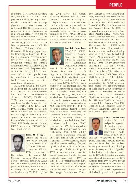
Toshiaki Masuhara<br />
(S768-M’69-SM’90-<br />
Fellow’94), Association<br />
<strong>of</strong> Super-<br />
Advanced Electronics<br />
Technologies<br />
(ASET), was born on<br />
Mar. 5, 1945 in Osaka, Japan. He<br />
obtained B.S., M.S. and Ph.D.<br />
degrees in Electrical Engineering<br />
from Kyoto University, Kyoto, Japan<br />
in 1967, 1969 and in 1977, respectively.<br />
From 1969 to 1974, he was a<br />
member <strong>of</strong> the technical staff, 3rd<br />
and 7th Department at Hitachi Central<br />
Research Laboratory(CRL),<br />
Kokubunji, Tokyo, Japan, where he<br />
worked on depletion-load NMOS<br />
integrated circuits and on modeling<br />
<strong>of</strong> sub-threshold characteristics <strong>of</strong><br />
MOS transistors. From 1974 to 1975,<br />
he was a special student, Department<br />
<strong>of</strong> Electrical Engineering and<br />
Computer Science, University <strong>of</strong><br />
California, Berkeley where he<br />
worked on double-diffused MOS<br />
transistors and a new CMOS<br />
process. In 1975, he returned to<br />
Hitachi CRL and worked on new<br />
high speed CMOS SRAM. In 1987,<br />
he became department manager,<br />
7th Dept., Hitachi CRL, developing<br />
memories, microprocessors, digital<br />
signal processors and high frequency<br />
silicon devices. He then became<br />
the manager <strong>of</strong> the 1st Dept. in<br />
1990, performing research on high<br />
speed GaAs and bipolar ICs and<br />
materials. From 1991 to 1993, he<br />
was in Telecommunications Division,<br />
Hitachi, where he was responsible<br />
for the design <strong>of</strong> telecom<br />
ICs.He became General Manager,<br />
Technology Development Opera-<br />
PEOPLE<br />
tion (Center) in 1993, General Manager,<br />
Semiconductor Manufacturing<br />
Technology Center, Semiconductor<br />
& IC Div. in 1997, and then became<br />
Senior Chief Engineer, Semiconductor<br />
Group, Hitachi. In 2001, he<br />
assumed his current position, Executive<br />
Director, MIRAI Project, Association<br />
<strong>of</strong> Super-Advanced Electronics<br />
Technologies (ASET).He is a<br />
member <strong>of</strong> <strong>IEEE</strong> and IEICE, Japan.<br />
He became a fellow <strong>of</strong> <strong>IEEE</strong> in 1994<br />
with the citation, ”For contribution<br />
in the invention and the development<br />
<strong>of</strong> NMOS circuits and highspeed<br />
CMOS memories”. He was<br />
the program co-chair and the chair<br />
in 1992-, 1993-, and general co-chair<br />
and chair in 1996- and 1997-VLSI<br />
Circuit Symposium. He was an<br />
elected member <strong>of</strong> the Administrative<br />
Committee, SSCS from 1998 to<br />
2000.He received <strong>IEEE</strong> Solid-State<br />
Circuit Technical Field Award on his<br />
contribution to NMOS depletionload<br />
circuits and the development<br />
<strong>of</strong> high speed CMOS memories in<br />
1990 and the <strong>IEEE</strong> third Millennium<br />
Medal in 2000. He has received a<br />
Significant Invention Award, Japan<br />
in 1994, four Significant Invention<br />
Awards, Tokyo, Japan in 1984, 1985,<br />
1988 and 1992, Significant Invention<br />
Awards, Yamanashi, Japan in 1995<br />
and Gumma, Japan in 1996.<br />
Akira Matsuzawa<br />
received B.S., M.S.,<br />
and ph. D. degrees in<br />
electronics engineering<br />
from Tohoku<br />
University, Sendai,<br />
Japan, in 1976, 1978,<br />
and 1997 respectively. In 1978, he<br />
joined Matsushita Electric Industrial<br />
Co., Ltd. Since then, he has been<br />
working on research and development<br />
<strong>of</strong> analog and Mixed Signal LSI<br />
technologies; ultra-high speed<br />
ADCs, RF CMOS circuits, and digital<br />
read-channel technologies for DVD<br />
systems. From 1997 to 2003, he was<br />
a general manager in advanced LSI<br />
technology development center. On<br />
April 2003, he joined Tokyo Institute<br />
<strong>of</strong> Technology and he is a pr<strong>of</strong>essor<br />
Winter 2007 <strong>IEEE</strong> SSCS NEWSLETTER 63


