

The Impact of Dennard's Scaling Theory - IEEE
The Impact of Dennard's Scaling Theory - IEEE
The Impact of Dennard's Scaling Theory - IEEE
- TAGS
- scaling
- www.ieee.org

Create successful ePaper yourself
Turn your PDF publications into a flip-book with our unique Google optimized e-Paper software.
RESEARCH HIGHLIGHTS<br />
Fig 2: Basic idea <strong>of</strong> noise cancelling; the noise due to M1<br />
is cancelled.<br />
noise. So we don't break the laws <strong>of</strong> physics: we still<br />
have to burn power (in amplifier “A”) to get a lownoise<br />
amplifier, but we have created a degree <strong>of</strong> freedom<br />
by decoupling the input matching (g m1 =1/Rs)<br />
and allowing a large gm ( g mA>>1/Rs) in the amplifier<br />
A. <strong>The</strong> noise <strong>of</strong> I bias is cancelled as well. A prototype<br />
amplifier has been realized on silicon and it worked<br />
well: the noise figure was well below 3dB, which<br />
proves the concept <strong>of</strong> noise canceling. Also the<br />
robustness to mismatch in the two noise paths is good<br />
[1]. Other topologies are also possible <strong>of</strong>fering “balun”<br />
functionality [1,2].<br />
Low Frequency noise reduction in MOSFETS<br />
Low frequency (LF) transistor noise, also denoted as<br />
1/f noise, is <strong>of</strong> great importance in today's circuit<br />
design. Especially, baseband circuits suffer from this<br />
noise phenomenon which can be dominant well<br />
above 10MHz. Also high-frequency oscillators suffer<br />
from LF noise, since this noise is up-converted and<br />
appears close to the carrier frequency <strong>of</strong> the oscillator<br />
degrading the close-in phase noise.<br />
A while ago, a MSc student Gian Hoogzaad did<br />
calculations on the phase noise <strong>of</strong> CMOS inverterbased<br />
ring oscillators. <strong>The</strong>se oscillators were free<br />
running, and we expected a large close-in phase<br />
noise due to the low frequency noise <strong>of</strong> the MOS-<br />
FETs in the oscillator. Measurements, however,<br />
showed a much lower, (8dB less), close-in phase<br />
noise than we expected from the LF noise <strong>of</strong> those<br />
single transistors. <strong>The</strong> student and his supervisor<br />
Sander Gierkink were very confident <strong>of</strong> his calculations,<br />
and we were thus wondering what caused the<br />
8dB lower close-in phase noise.<br />
Finally, we suspected that the large signal switching<br />
behavior in the inverters caused the strange effect<br />
and we carried out measurements on stand-alone<br />
transistors under normal bias and under “switched<br />
bias”. Figure 3 illustrates these conditions.<br />
One would expect 6 dB less noise from the<br />
switched bias transistors compared to the normal one:<br />
3dB reduction due to the 50% duty-cycle <strong>of</strong> the noise<br />
and another 3dB due to up-conversion <strong>of</strong> the LF noise.<br />
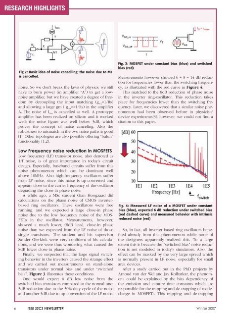
Fig. 3: MOSFET under constant bias (blue) and switched<br />
bias (red)<br />
Measurements however showed 6 + 8 = 14 dB reduction<br />
for frequencies lower than the switching frequency,<br />
as illustrated with the red curve in Figure 4.<br />
This matched to the 8dB reduction <strong>of</strong> phase noise<br />
in the inverter ring-oscillator. This reduction takes<br />
place for frequencies lower than the switching frequency.<br />
Later, we discovered that a similar noise phenomenon<br />
had been observed before in physicists'<br />
device experiments[3]; however, we could not find a<br />
citation to this paper.<br />
Fig. 4: Measured LF noise <strong>of</strong> a MOSFET under constant<br />
bias (blue), expected 6 dB reduction under switched bias<br />
(red dashed curve) and measured behavior with intrinsic<br />
reduced noise (red)<br />
So, in fact, all inverter based ring oscillators benefited<br />
already from this phenomenon while none <strong>of</strong><br />
the designers apparently realized this. To a large<br />
extent this is because the “switched bias” noise reduction<br />
is not modeled in today's simulators. Also, the<br />
effect can be masked by the very large spread which<br />
is normally present in LF noise, especially for small<br />
area devices.<br />
After a study carried out in the PhD projects by<br />
Arnoud van der Wel and Jay Kolhatkar, the phenomena<br />
could be explained by the bias dependency <strong>of</strong><br />
the emission and capture time constants which are<br />
responsible for the trapping and de-trapping <strong>of</strong> oxidecharge<br />
in MOSFETs. This trapping and de-trapping<br />
6 <strong>IEEE</strong> SSCS NEWSLETTER Winter 2007

