

The Impact of Dennard's Scaling Theory - IEEE
The Impact of Dennard's Scaling Theory - IEEE
The Impact of Dennard's Scaling Theory - IEEE
- TAGS
- scaling
- www.ieee.org

You also want an ePaper? Increase the reach of your titles
YUMPU automatically turns print PDFs into web optimized ePapers that Google loves.
TECHNICAL ARTICLES<br />
overhead <strong>of</strong> the input/output structures, the scribe<br />
lane, etc. If the die size gets too big, the cost per gate<br />
increases due to the increased complexity. For simplicity,<br />
gate count is assumed here to be an equivalent<br />
2-input NAND gate count. Each equivalent gate<br />
uses four transistors. <strong>The</strong> optimum gate density and<br />
cost per gate can be converted to transistor density<br />
and cost per transistor. <strong>The</strong> actual transistor count per<br />
chip increases rapidly as larger amounts <strong>of</strong> memory is<br />
included on the die. For reference, one <strong>of</strong> Intel’s Pentium<br />
processors is reported with 55M transistors (14M<br />
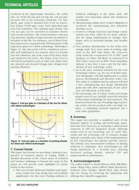
equivalent gates) in a 90nm technology 4. Referring to<br />
Figure 10, this data point will be considered reasonably<br />
well optimized in our analysis, since it is located<br />
near the minimum, just at the cusp <strong>of</strong> the steep slope<br />
and marked by the arrow. <strong>The</strong> shape <strong>of</strong> the curve is<br />
affected by parameters such as wafer cost, defect density,<br />
physical and electrical design rules, design tools’<br />
packing efficiency.<br />
cents/KGates<br />
Figure 9 Cost per gate as a function <strong>of</strong> die size for 90nm<br />
and 180nm technologies<br />
cents/KGates<br />
Figure 10 Cost per gate as a function <strong>of</strong> packing density<br />
for 90nm and 180nm technologies<br />
7. Current Trends<br />
This paper has focused on providing a historical perspective<br />
<strong>of</strong> business aspects <strong>of</strong> scaling. While a<br />
detailed discussion <strong>of</strong> the current status <strong>of</strong> technical<br />
and business challenges is beyond the scope <strong>of</strong> this<br />
paper, we will provide some highlights <strong>of</strong> current<br />
trends in this section.<br />
a. <strong>The</strong> cost <strong>of</strong> wafer fabrication facilities and equipment,<br />
masks and chip design have all escalated<br />
significantly over the years. Finding solutions to<br />
technical challenges at the 32nm node will<br />
require ever increasing capital and manpower<br />
investments.<br />
b. Manufacturing entities have worked diligently to<br />
accelerate the manufacturing and defectivity<br />
learning curves.<br />
c. Creative co-design <strong>of</strong> process and design considerations<br />
has been called for by many authors 10<br />
and are being implemented to manage challenges<br />
such as increased leakage and standby<br />
power.<br />
d. New product introductions on the 65nm technology<br />
node have been made at leading edge<br />
users in the 2005 time frame; the cross-over<br />
point varies but is expected to be in 2007. Lead<br />
products on 45nm will likely be announced in<br />
2007 with a cross-over in 2009. <strong>The</strong>se timetables<br />
indicate a less than 3 year cycle for the introduction<br />
<strong>of</strong> new technology nodes.<br />
e. As in the past, technical solutions for the next<br />
technology (32nm), e.g. the use <strong>of</strong> double-exposure<br />
lithography, will add significantly to capital,<br />
process development and therefore wafer cost.<br />
<strong>The</strong> author is confident that the industry will find<br />
a new manufacturing and design optimization<br />
point that will allow introduction <strong>of</strong> new products<br />
cost-effectively at this node.<br />
f. <strong>The</strong> increasing cost <strong>of</strong> wafers, masks and design<br />
require users to very carefully assess the selection<br />
<strong>of</strong> the proper technology for their products. <strong>The</strong><br />
trend is towards the use <strong>of</strong> leading edge technology<br />
nodes only for products with very high volumes,<br />
a compelling technical argument and a<br />
clear value proposition.<br />
8. Summary<br />
This paper has provided a simplified view <strong>of</strong> the<br />
business aspects <strong>of</strong> scaling and technology migrations<br />
that have been key to sustaining a phenomenal<br />
reduction in CPF for integrated circuits. Although<br />
trends such as the increasing cost <strong>of</strong> wafer fabs,<br />
masks and the increasing cost <strong>of</strong> complex designs<br />
indicate a possible slow down <strong>of</strong> the implementation<br />
<strong>of</strong> new technologies, the industry marches onward.<br />
<strong>The</strong> industry has demonstrated resilience in finding<br />
solutions to challenges. New technologies are still<br />
being introduced at a feverish pace allowing<br />
increased packing density, reduced CPF and<br />
improvements in performance.<br />
9. Acknowledgements<br />
<strong>The</strong> author wishes to thank Behrooz Abdi, Bill Bidermann,<br />
Mung Chen, James Clifford, Brian Henderson,<br />
Pr<strong>of</strong>essor Dave Hodges, Merrill Hunt, Matt Nowak<br />
and Ian Young for reviewing the manuscript and<br />
<strong>of</strong>fering their valuable suggestions.<br />
26 <strong>IEEE</strong> SSCS NEWSLETTER Winter 2007

