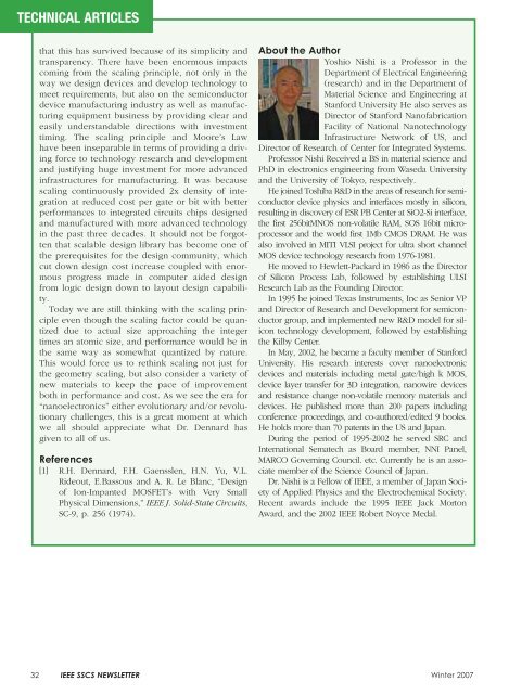
The Impact of Dennard's Scaling Theory - IEEE
The Impact of Dennard's Scaling Theory - IEEE
The Impact of Dennard's Scaling Theory - IEEE
- TAGS
- scaling
- www.ieee.org
Create successful ePaper yourself
Turn your PDF publications into a flip-book with our unique Google optimized e-Paper software.
TECHNICAL ARTICLES<br />
that this has survived because <strong>of</strong> its simplicity and<br />
transparency. <strong>The</strong>re have been enormous impacts<br />
coming from the scaling principle, not only in the<br />
way we design devices and develop technology to<br />
meet requirements, but also on the semiconductor<br />
device manufacturing industry as well as manufacturing<br />
equipment business by providing clear and<br />
easily understandable directions with investment<br />
timing. <strong>The</strong> scaling principle and Moore’s Law<br />
have been inseparable in terms <strong>of</strong> providing a driving<br />
force to technology research and development<br />
and justifying huge investment for more advanced<br />
infrastructures for manufacturing. It was because<br />
scaling continuously provided 2x density <strong>of</strong> integration<br />
at reduced cost per gate or bit with better<br />
performances to integrated circuits chips designed<br />
and manufactured with more advanced technology<br />
in the past three decades. It should not be forgotten<br />
that scalable design library has become one <strong>of</strong><br />
the prerequisites for the design community, which<br />
cut down design cost increase coupled with enormous<br />
progress made in computer aided design<br />
from logic design down to layout design capability.<br />
Today we are still thinking with the scaling principle<br />
even though the scaling factor could be quantized<br />
due to actual size approaching the integer<br />
times an atomic size, and performance would be in<br />
the same way as somewhat quantized by nature.<br />
This would force us to rethink scaling not just for<br />
the geometry scaling, but also consider a variety <strong>of</strong><br />
new materials to keep the pace <strong>of</strong> improvement<br />
both in performance and cost. As we see the era for<br />
“nanoelectronics” either evolutionary and/or revolutionary<br />
challenges, this is a great moment at which<br />
we all should appreciate what Dr. Dennard has<br />
given to all <strong>of</strong> us.<br />
References<br />
[1] R.H. Dennard, F.H. Gaensslen, H.N. Yu, V.L.<br />
Rideout, E.Bassous and A. R. Le Blanc, “Design<br />
<strong>of</strong> Ion-Impanted MOSFET’s with Very Small<br />
Physical Dimensions,” <strong>IEEE</strong> J. Solid-State Circuits,<br />
SC-9, p. 256 (1974).<br />
About the Author<br />
Yoshio Nishi is a Pr<strong>of</strong>essor in the<br />
Department <strong>of</strong> Electrical Engineering<br />
(research) and in the Department <strong>of</strong><br />
Material Science and Engineering at<br />
Stanford University He also serves as<br />
Director <strong>of</strong> Stanford Nan<strong>of</strong>abrication<br />
Facility <strong>of</strong> National Nanotechnology<br />
Infrastructure Network <strong>of</strong> US, and<br />
Director <strong>of</strong> Research <strong>of</strong> Center for Integrated Systems.<br />
Pr<strong>of</strong>essor Nishi Received a BS in material science and<br />
PhD in electronics engineering from Waseda University<br />
and the University <strong>of</strong> Tokyo, respectively.<br />
He joined Toshiba R&D in the areas <strong>of</strong> research for semiconductor<br />
device physics and interfaces mostly in silicon,<br />
resulting in discovery <strong>of</strong> ESR PB Center at SiO2-Si interface,<br />
the first 256bitMNOS non-volatile RAM, SOS 16bit microprocessor<br />
and the world first 1Mb CMOS DRAM. He was<br />
also involved in MITI VLSI project for ultra short channel<br />
MOS device technology research from 1976-1981.<br />
He moved to Hewlett-Packard in 1986 as the Director<br />
<strong>of</strong> Silicon Process Lab, followed by establishing ULSI<br />
Research Lab as the Founding Director.<br />
In 1995 he joined Texas Instruments, Inc as Senior VP<br />
and Director <strong>of</strong> Research and Development for semiconductor<br />
group, and implemented new R&D model for silicon<br />
technology development, followed by establishing<br />
the Kilby Center.<br />
In May, 2002, he became a faculty member <strong>of</strong> Stanford<br />
University. His research interests cover nanoelectronic<br />
devices and materials including metal gate/high k MOS,<br />
device layer transfer for 3D integration, nanowire devices<br />
and resistance change non-volatile memory materials and<br />
devices. He published more than 200 papers including<br />
conference proceedings, and co-authored/edited 9 books.<br />
He holds more than 70 patents in the US and Japan.<br />
During the period <strong>of</strong> 1995-2002 he served SRC and<br />
International Sematech as Board member, NNI Panel,<br />
MARCO Governing Council. etc. Currently he is an associate<br />
member <strong>of</strong> the Science Council <strong>of</strong> Japan.<br />
Dr. Nishi is a Fellow <strong>of</strong> <strong>IEEE</strong>, a member <strong>of</strong> Japan Society<br />
<strong>of</strong> Applied Physics and the Electrochemical Society.<br />
Recent awards include the 1995 <strong>IEEE</strong> Jack Morton<br />
Award, and the 2002 <strong>IEEE</strong> Robert Noyce Medal.<br />
32 <strong>IEEE</strong> SSCS NEWSLETTER Winter 2007


