

The Impact of Dennard's Scaling Theory - IEEE
The Impact of Dennard's Scaling Theory - IEEE
The Impact of Dennard's Scaling Theory - IEEE
- TAGS
- scaling
- www.ieee.org

You also want an ePaper? Increase the reach of your titles
YUMPU automatically turns print PDFs into web optimized ePapers that Google loves.
Fig. 3. Experimental turn-on characteristics for conventional<br />
and scaled-down devices shown in Fig. 1 normalized to<br />
W/L =1.<br />
One area in which the device characteristics fail to<br />
scale is in the subthreshold or weak inversion region<br />
<strong>of</strong> the turn-on characteristic. Below threshold, Id is<br />
exponentially dependent on Vg with an inverse semilogarithmic<br />
slope, α, [10], [11] which for the scaleddown<br />
device is given by<br />
α ′<br />
� �<br />
volts<br />
=<br />
decade<br />
dVg ′<br />
d log 10 Id ′<br />
= (kT/q log 10 e)<br />
�<br />
1 + ɛSitox/κ<br />
�<br />
, (4)<br />
ɛoxwd /κ<br />
which is the same as for the original larger device.<br />
<strong>The</strong> parameter α is important to dynamic memory circuits<br />
because it determines the gate voltage excursion<br />
required to go from the low current “<strong>of</strong>f” state to the<br />
high current “on” state [11]. In an attempt to also<br />
extend the linear scaling relationships to α one could<br />
reduce the operating temperature in (4) (i.e.,<br />
T ′ = T/κ, but this would cause a significant increase<br />
in the effective surface mobility [12] and thereby invalidate<br />
the current scaling relationship <strong>of</strong> (3). In order<br />
to design devices for operation at room temperature<br />
and above, one must accept the fact that the subthreshold<br />
behavior does not scale as desired. This<br />
nonscaling property <strong>of</strong> the subthreshold characteristic<br />
is <strong>of</strong> particular concern to miniature dynamic memory<br />
circuits which require low source-to-drain leakage<br />
currents.<br />
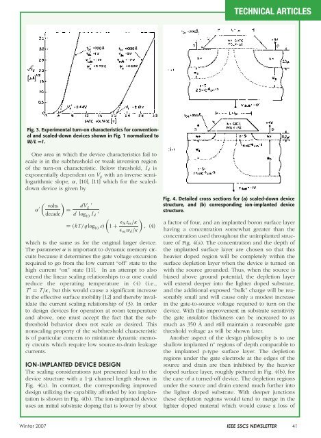
ION-IMPLANTED DEVICE DESIGN<br />
<strong>The</strong> scaling considerations just presented lead to the<br />
device structure with a 1-μ channel length shown in<br />
Fig. 4(a). In contrast, the corresponding improved<br />
design utilizing the capability afforded by ion implantation<br />
is shown in Fig. 4(b). <strong>The</strong> ion-implanted device<br />
uses an initial substrate doping that is lower by about<br />
TECHNICAL ARTICLES<br />
Fig. 4. Detailed cross sections for (a) scaled-down device<br />
structure, and (b) corresponding ion-implanted device<br />
structure.<br />
a factor <strong>of</strong> four, and an implanted boron surface layer<br />
having a concentration somewhat greater than the<br />
concentration used throughout the unimplanted structure<br />
<strong>of</strong> Fig. 4(a). <strong>The</strong> concentration and the depth <strong>of</strong><br />
the implanted surface layer are chosen so that this<br />
heavier doped region will be completely within the<br />
surface depletion layer when the device is turned on<br />
with the source grounded. Thus, when the source is<br />
biased above ground potential, the depletion layer<br />
will extend deeper into the lighter doped substrate,<br />
and the additional exposed “bulk” charge will be reasonably<br />
small and will cause only a modest increase<br />
in the gate-to-source voltage required to turn on the<br />
device. With this improvement in substrate sensitivity<br />
the gate insulator thickness can be increased to as<br />
much as 350 Å and still maintain a reasonable gate<br />
threshold voltage as will be shown later.<br />
Another aspect <strong>of</strong> the design philosophy is to use<br />
shallow implanted n + regions <strong>of</strong>’ depth comparable to<br />
the implanted p-type surface layer. <strong>The</strong> depletion<br />
regions under the gate electrode at the edges <strong>of</strong> the<br />
source and drain are then inhibited by the heavier<br />
doped surface layer, roughly pictured in Fig. 4(b), for<br />
the case <strong>of</strong> a turned-<strong>of</strong>f device. <strong>The</strong> depletion regions<br />
under the source and drain extend much further into<br />
the lighter doped substrate. With deeper junctions<br />
these depletion regions would tend to merge in the<br />
lighter doped material which would cause a loss <strong>of</strong><br />
Winter 2007 <strong>IEEE</strong> SSCS NEWSLETTER 41

