

The Impact of Dennard's Scaling Theory - IEEE
The Impact of Dennard's Scaling Theory - IEEE
The Impact of Dennard's Scaling Theory - IEEE
- TAGS
- scaling
- www.ieee.org

You also want an ePaper? Increase the reach of your titles
YUMPU automatically turns print PDFs into web optimized ePapers that Google loves.
TECHNICAL ARTICLES<br />
Such technology scaling was achieved typically in<br />
the following manner:<br />
a. Drive new photo lithography equipment and<br />
processes that allowed printing and patterning <strong>of</strong><br />
dimensions 30% smaller than in the previous<br />
generation.<br />
b. Make improvements to other parts <strong>of</strong> the<br />
process, e.g., gate oxidation, ion implantation,<br />
diffusion, etching, interconnect metallurgy etc.<br />
c. Engineer and optimize the transistor device<br />
structure and various aspects <strong>of</strong> the process to<br />
meet performance and cost goals, and be manufacturable<br />
and reliable.<br />
d. Execute a “Linear Shrink” <strong>of</strong> an existing product<br />
reducing the die size by a scaling factor such<br />
as 0.7. Due to various intricacies <strong>of</strong> the process,<br />
the design rules and device characteristics at<br />
shrinking geometries, such scaling became<br />
increasingly difficult. In the mid-1980’s such an<br />
approach, which was referred to by some people<br />
as a “dumb shrink” became known as an<br />
“intelligent laborious shrink” at some companies.<br />
e. A new set <strong>of</strong> design rules - both physical and<br />
electrical - were usually used to design new<br />
products that took full advantage <strong>of</strong> the new<br />
technology capability. While the shrink approach<br />
was able to get an initial product out in the new<br />
technology node, the “Re-Design” approach was<br />
necessary to maximize performance and minimize<br />
cost <strong>of</strong> products in the new node.<br />
f. In addition, the new technology usually had some<br />
new features aimed at increasing the packing efficiency,<br />
design productivity and device performance.<br />
Some examples are: increasing the number<br />
<strong>of</strong> metal interconnect layers, self-aligned polysilicon<br />
gate structure, oxide and trench isolation,<br />
standard cells, EDA tools and re-usable IP blocks.<br />
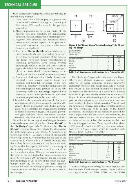
We will now discuss migration <strong>of</strong> designs from one<br />
node to the next using either the “Linear Shrink” or<br />
the “Re-Design” approach. To illustrate the “Linear<br />
Shrink”, consider Figure 4(a), which depicts a square<br />
die with dimension y and having N transistors, in<br />
technology node T1. A simple shrink <strong>of</strong> the die into<br />
technology node T2 would reduce the die size by the<br />
scale factor k, where 0

