

The Impact of Dennard's Scaling Theory - IEEE
The Impact of Dennard's Scaling Theory - IEEE
The Impact of Dennard's Scaling Theory - IEEE
- TAGS
- scaling
- www.ieee.org

Create successful ePaper yourself
Turn your PDF publications into a flip-book with our unique Google optimized e-Paper software.
TECHNICAL ARTICLES<br />
Ion Implanted MOSFET’s With Very Short Channel<br />
Lengths<br />
R. H. Dennard, F. H. Gaensslen, H. N. Yu, V. L. Rideout, E. Bassous , and A. LeBlanc<br />
IBM Thomas J. Watson Research Center, Yorktown Heights, N. Y.<br />
Copyright 1973 <strong>IEEE</strong>. Reprinted with permission. Technical Digest, <strong>IEEE</strong> International Electron Devices Meeting, 1973, pp. 152-155.<br />
It has been shown previously that MOSFET switching<br />
devices can be scaled down to have one micron spacing<br />
between source and drain. In order to achieve<br />
electrical characteristics suitable for dynamic memory and<br />
other digital applications, such miniaturized devices must<br />
have reduced gate insulator thickness and junction depth,<br />
reduced operating voltages, and increased substrate doping<br />
(1). <strong>The</strong> previously described one micron device<br />
structure is shown in Fig.1(a). With uniform substrate<br />
doping, a 200°A gate insulator is required to achieve the<br />
desired control <strong>of</strong> the gate threshold voltage over the<br />
operating range <strong>of</strong> the source and drain voltages.<br />
Figure 1: MOS device designs for micron source-drain<br />
spacing. (a) Unimplanted design (b)Design with ion<br />
implantation.<br />
<strong>The</strong> present paper addresses improvements in the<br />
design <strong>of</strong> micron devices which can be obtained by<br />
using ion implantation. <strong>The</strong> new n-channel design,<br />
which is shown in Fig. 1(b), uses a lighter doped substrate<br />
with a relatively heavy doped p-type region at the<br />
surface between the source and drain. This implanted ptype<br />
region gives the desired threshold magnitude, and<br />
also controls the extent <strong>of</strong> the source and drain depletion<br />
regions beneath the gate. With the gate turned <strong>of</strong>f,<br />
these depletion regions must be kept separated so that<br />
the surface potential in the channel region is indeed<br />
controlled by the gate. Merging <strong>of</strong> the depletion layers<br />
in the lighter doped substrate is prevented by using shallow<br />
implanted source and drain junctions <strong>of</strong> depth comparable<br />
to the p-type implanted region, and also by<br />
choice <strong>of</strong> a moderate substrate doping level.<br />
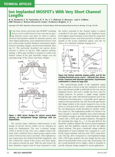
Figure 2(a) Vertical substrate doping pr<strong>of</strong>ile, and (b) the<br />
resulting threshold versus source - substrate bias characteristic<br />
compared with alternate approaches. Experimental<br />
confirmation is shown by large dots.<br />
<strong>The</strong> vertical-doping pr<strong>of</strong>ile <strong>of</strong> the implanted region<br />
beneath the gate is shown in Fig. 2(a). Intuitively, it was felt<br />
that a step function pr<strong>of</strong>ile is preferable for the one micron<br />
implanted device, and such a pr<strong>of</strong>ile has been used for<br />
design purposes. In practice a single energy implant<br />
through the gate oxide with thermal treatment used in the<br />
subsequent processing gives a reasonably good approximation<br />
to the step function. Fig. 2(b) shows the gate threshold<br />
voltage (relative to the source) required to turn on the<br />
device as a function <strong>of</strong> the source - substrate potential using<br />
the one-dimensional model described in another conference<br />
paper (2). <strong>The</strong> implantation pr<strong>of</strong>ile was chosen to be<br />
deep enough to prevent depletion layer punch through,<br />
and shallow enough to give the desired threshold voltage<br />
control with a 350°A gate insulator thickness. Throughout<br />
the operating bias range (Vs-sub > 1), the gate field for the<br />
threshold condition depletes the heavier doped implanted<br />
region, and this depletion extends well into the lighter<br />
doped substrate. This gives a threshold voltage relatively<br />
independent <strong>of</strong> source-substrate bias compared to a uniformly<br />
doped substrate with the same 350°A oxide thickness.<br />
(See Fig. 2(b)). Compared to a non-implanted design<br />
with a 200°A gate insulator, the new design has the same<br />
slope in the threshold versus source bias characteristic, but<br />
the overall threshold level is higher, which is desirable to<br />
provide adequate design margins for circuit applications.<br />
36 <strong>IEEE</strong> SSCS NEWSLETTER Winter 2007

