

The Impact of Dennard's Scaling Theory - IEEE
The Impact of Dennard's Scaling Theory - IEEE
The Impact of Dennard's Scaling Theory - IEEE
- TAGS
- scaling
- www.ieee.org

Create successful ePaper yourself
Turn your PDF publications into a flip-book with our unique Google optimized e-Paper software.
TECHNICAL ARTICLES<br />
In (2) the reduction in Vt is primarily due to the<br />
decreased insulator thickness, tox/κ, while the<br />
changes in the voltage and doping terms tend to cancel<br />
out. In most cases <strong>of</strong> interest (i.e., polysilicon<br />
gates <strong>of</strong> doping type opposite to that <strong>of</strong> the substrate<br />
or aluminum gates on p-type substrates) the work<br />
function difference �W f is <strong>of</strong> opposite sign, and<br />
approximately cancels out ψs ′ . ψs ′ is the band<br />
bending in the silicon (i.e., the surface potential) at<br />
the onset <strong>of</strong> strong inversion for zero substrate bias. It<br />
would appear that the ψ ′ terms appearing in (1) and<br />
(2) prevent exact scaling since they remain approximately<br />
constant, actually increasing slightly due to the<br />
increased doping since ψb ′ � ψs ′ = (2kT/q) ln<br />
(Na ′ /ni). However, the fixed substrate bias supply<br />
normally used with n-channel devices can be adjusted<br />
so that (ψs ′ + Vsub ′ ) = (ψs + Vsub)/κ . Thus, by<br />
scaling down the applied substrate bias more than the<br />
other applied voltages, the potential drop across the<br />
source or drain junctions, or across the depletion<br />
region under the gate, can he reduced by κ.<br />
All <strong>of</strong> the equations that describe the MOSFET<br />
device characteristics may be scaled as demonstrated<br />
above. For example, the MOSFET current equation [9]<br />
given by<br />
Id ′ = μeffɛox<br />
tox/κ<br />
� �� �<br />
W /κ Vg − Vt − Vd /2<br />
·<br />
L/κ κ<br />
(Vd /κ) = Id /κ (3)<br />
is seen to be reduced by a factor <strong>of</strong> κ, for any given<br />
set <strong>of</strong> applied voltages, assuming no change in mobility.<br />
Actually, the mobility is reduced slightly due to<br />
increased impurity scattering in the heavier doped<br />
substrate.<br />
It is possible to generalize the scaling approach to<br />
include electric field patterns and current density. <strong>The</strong><br />
electric field distribution is maintained in the scaleddown<br />
device except for a change in scale for the spatial<br />
coordinates. Furthermore, the electric field<br />
strength at any corresponding point is unchanged<br />
because V /x = V ′ /x ′ . Thus, the carrier velocity at any<br />
point is also unchanged due to scaling and, hence,<br />
any saturation velocity effects will be similar in both<br />
devices, neglecting microscopic differences due to the<br />
fixed crystal lattice dimensions. From (3), since the<br />
device current is reduced by κ, the channel current<br />
per unit <strong>of</strong> channel width W is unchanged by scaling.<br />
This is consistent with the same sheet density <strong>of</strong> carriers<br />
(i.e., electrons per unit gate area) moving at the<br />
same velocity. In the vicinity <strong>of</strong> the drain, the carriers<br />
will move away from the surface to a lesser extent in<br />
the new device, due to the shallower diffusions. Thus,<br />
the density <strong>of</strong> mobile carriers per unit volume will be<br />
higher in the space-charge region around the drain,<br />
complementing the higher density <strong>of</strong> immobile charge<br />
due to the heavier doped substrate. Other scaling<br />
relationships for power density, delay time, etc., are<br />
given in Table I and will be discussed in a subsequent<br />
section on circuit performance.<br />
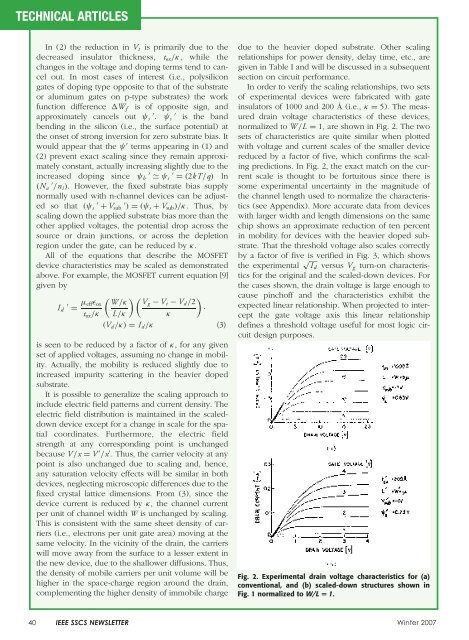
In order to verify the scaling relationships, two sets<br />
<strong>of</strong> experimental devices were fabricated with gate<br />
insulators <strong>of</strong> 1000 and 200 Å (i.e., κ = 5). <strong>The</strong> measured<br />
drain voltage characteristics <strong>of</strong> these devices,<br />
normalized to W /L = 1, are shown in Fig. 2. <strong>The</strong> two<br />
sets <strong>of</strong> characteristics are quite similar when plotted<br />
with voltage and current scales <strong>of</strong> the smaller device<br />
reduced by a factor <strong>of</strong> five, which confirms the scaling<br />
predictions. In Fig. 2, the exact match on the current<br />
scale is thought to be fortuitous since there is<br />
some experimental uncertainty in the magnitude <strong>of</strong><br />
the channel length used to normalize the characteristics<br />
(see Appendix). More accurate data from devices<br />
with larger width and length dimensions on the same<br />
chip shows an approximate reduction <strong>of</strong> ten percent<br />
in mobility for devices with the heavier doped substrate.<br />
That the threshold voltage also scales correctly<br />
by a factor <strong>of</strong> five is verified in Fig. 3, which shows<br />
the experimental √ Id versus Vg turn-on characteristics<br />
for the original and the scaled-down devices. For<br />
the cases shown, the drain voltage is large enough to<br />
cause pinch<strong>of</strong>f and the characteristics exhibit the<br />
expected linear relationship. When projected to intercept<br />
the gate voltage axis this linear relationship<br />
defines a threshold voltage useful for most logic circuit<br />
design purposes.<br />
Fig. 2. Experimental drain voltage characteristics for (a)<br />
conventional, and (b) scaled-down structures shown in<br />
Fig. 1 normalized to W/L = 1.<br />
40 <strong>IEEE</strong> SSCS NEWSLETTER Winter 2007

