

The Impact of Dennard's Scaling Theory - IEEE
The Impact of Dennard's Scaling Theory - IEEE
The Impact of Dennard's Scaling Theory - IEEE
- TAGS
- scaling
- www.ieee.org

You also want an ePaper? Increase the reach of your titles
YUMPU automatically turns print PDFs into web optimized ePapers that Google loves.
TECHNICAL ARTICLES<br />
threshold control or, in the extreme, punchthrough at<br />
high drain voltages. However, the shallower junctions<br />
give a more favorable electric field pattern which<br />
avoids these effects when the substrate doping concentration<br />
is properly chosen (i.e., when it is not too<br />
light).<br />
<strong>The</strong> device capacitances are reduced with the ionimplanted<br />
structure due to the increased depletion<br />
layer width separating the source and drain from the<br />
substrate [cf. Figs. 4(a) and 4(b)], and due to the natural<br />
self-alignment afforded by the ion implantation<br />
process which reduces the overlap <strong>of</strong> the polysilicon<br />
gate over the source and drain regions. <strong>The</strong> thicker<br />
gate insulator also gives reduced gate capacitance, but<br />
the performance benefit in this respect is <strong>of</strong>fset by the<br />
decreased gate field. To compensate for the thicker<br />
gate oxide and the expected threshold increase, a<br />
design objective for maximum drain voltage was set<br />
at 4 V for the ion-implanted design in Fig. 4(b), compared<br />
to 3 V for the scaled-down device <strong>of</strong> Fig.4(a).<br />
FABRICATION OF ION-IMPLANTED MOSFET’s<br />
<strong>The</strong> fabrication process for the ion-implanted MOS-<br />
FET’s used in this study will now be described. A<br />
four-mask process was used to fabricate polysilicongate,<br />
n-channel MOSFET’s on a test chip which contains<br />
devices with channel lengths ranging from 0.5 to<br />
10 μ. Though the eventual aim is to use electronbeam<br />
pattern exposure, it was more convenient to<br />
use contact masking with high quality master masks<br />
for process development. For this purpose high resolution<br />
is required only for the gate pattern which uses<br />
lines as small as 1.5 μ which are reduced in the subsequent<br />
processing. <strong>The</strong> starting substrate resistivity<br />
was 2 �·cm (i.e., about 7.5 × 10 15 cm −3 ). <strong>The</strong> method<br />
<strong>of</strong> fabrication for the thick oxide isolation between<br />
adjacent FET’s is not described as it is not essential to<br />
the work presented here, and because several suitable<br />
techniques are available. Following dry thermal<br />
growth <strong>of</strong> the gate oxide, low energy (40 keV), low<br />
dose (6.7 × 10 11 atoms/cm 2 ) B 11 ions were implanted<br />
into the wafers, raising the boron doping near the silicon<br />
surface. All implantations were performed after<br />
gate oxide growth in order to restrict diffusion <strong>of</strong> the<br />
implanted regions.<br />
After the channel implantation, a 3500-Å thick polysilicon<br />
layer was deposited, doped n + , and the gate<br />
regions delineated. Next, n + source and drain regions<br />
2000-Å deep were formed by a high energy (100<br />
keV), high dose (4 × 10 15 atoms/cm 2 ) As 75 implantation<br />
through the same 350-Å oxide layer. During this<br />
step, however, the polysilicon gate masks the channel<br />
region from the implant, absorbing all <strong>of</strong> the As 75<br />
dose incident there. <strong>The</strong> etching process used to<br />
delineate the gates results in a sloping sidewall which<br />
allows a slight penetration <strong>of</strong> As 75 ions underneath<br />
the edges <strong>of</strong> the gates. <strong>The</strong> gate-to-drain (or source)<br />
overlap is estimated to be <strong>of</strong> the order <strong>of</strong> 0.2 μ. <strong>The</strong><br />
high temperature processing steps that follow the<br />
implantations include 20 min at 900°C, and 11 min at<br />
1000°C, which is more than adequate to anneal out<br />
the implantation damage without greatly spreading<br />
out the implanted doses. Typical sheet resistances<br />
were 50�/� for the source and drain regions, and<br />
40�/� for the polysilicon areas. Following the As 75<br />
implant, a final insulating oxide layer 2000-Å thick<br />
was deposited using low-temperature chemical-vapor<br />
deposition. <strong>The</strong>n, the contact holes to the n + and<br />
polysilicon regions were defined, and the metalization<br />
was applied and delineated. Electrical contact directly<br />
to the shallow implanted source and drain regions<br />
was accomplished by a suitably chosen metallurgy to<br />
avoid junction penetration due to alloying during the<br />
final annealing step. After metalization an annealing<br />
step <strong>of</strong> 400 °C for 20 min in forming gas was performed<br />
to decrease the fast-state density.<br />
ONE-DIMENSIONAL (LONG CHANNEL)<br />
ANALYSIS<br />
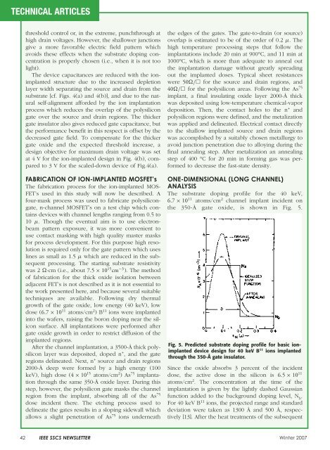
<strong>The</strong> substrate doping pr<strong>of</strong>ile for the 40 keV,<br />
6.7 × 10 11 atoms/cm 2 channel implant incident on<br />
the 350-Å gate oxide, is shown in Fig. 5.<br />
Fig. 5. Predicted substrate doping pr<strong>of</strong>ile for basic ionimplanted<br />
device design for 40 keV B 11 ions implanted<br />
through the 350-Å gate insulator.<br />
Since the oxide absorbs 3 percent <strong>of</strong> the incident<br />
dose, the active dose in the silicon is 6.5 × 10 11<br />
atoms/cm 2 . <strong>The</strong> concentration at the time <strong>of</strong> the<br />
implantation is given by the lightly dashed Gaussian<br />
function added to the background doping level, N b .<br />
For 40 keV B 11 ions, the projected range and standard<br />
deviation were taken as 1300 Å and 500 Å, respectively<br />
[13]. After the heat treatments <strong>of</strong> the subsequent<br />
42 <strong>IEEE</strong> SSCS NEWSLETTER Winter 2007

