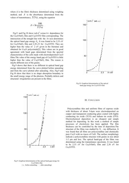
- Page 1 and 2:
Project logo: Priority logo: Projec
- Page 3 and 4:
Paper Session 6 thBALKAN POWER CONF
- Page 5 and 6:
6 thBALKAN POWER CONFERENCE Panel S
- Page 7 and 8:
- WAYS TO MINIMIZE THE GREENHOUSE G
- Page 9 and 10:
BPC 2006 INTRODUCTION • The inter
- Page 11 and 12:
CARBON EMISSIONS TRADING - A NEW WE
- Page 13 and 14:
CARBON EMISSIONS TRADING - A NEW WE
- Page 15 and 16:
PROMOTION OF RENEWABLE RESOURCES
- Page 17 and 18:
NUCLEAR POWER - NOT ONLY AN OPTION,
- Page 19 and 20:
ROMANIAN APPROACH BPC 2006 • In 2
- Page 21 and 22:
ROMANIAN APPROACH BPC 2006 The tren
- Page 23 and 24:
ROMANIAN APPROACH BPC 2006 • The
- Page 25 and 26:
ROMANIAN APPROACH BPC 2006 • Anot
- Page 27 and 28:
CONCLUSIONS BPC 2006 • We conside
- Page 29 and 30:
ioan.manicuta@opcom.ro
- Page 31 and 32:
kategorizicija na hidrogeotermalnit
- Page 33 and 34:
konduktivni hidrogeotermalni sistem
- Page 35 and 36:
Glavni geotermalni poliwa vo Makedo
- Page 37 and 38:
metodi za odreduvawe na geotermalni
- Page 39 and 40:
U~estvo na poedine~ni energenti vo
- Page 41 and 42:
PREPORAKI so relativno mali vlo`uv
- Page 43 and 44:
6th Balkan Power Conference Romania
- Page 45 and 46:
Electricity are traded separately f
- Page 47 and 48:
Support system for E-RES E RES Fixe
- Page 49 and 50:
Central Central Command Command and
- Page 51 and 52:
CGCMO determines: determines determ
- Page 53 and 54:
10.000 10.000 9.000 9.000 8.000 8.0
- Page 55 and 56:
50 50 45 45 40 40 35 35 30 30 25 25
- Page 57 and 58:
Centralized Green Certificates Mark
- Page 59 and 60:
90 90 80 80 70 70 60 60 50 50 40 40
- Page 61 and 62:
Thank you for your attention Ghergh
- Page 63 and 64:
ABSTRACT Biomass is one of the very
- Page 65 and 66:
INTRODUCTION -Biogas is a mixture o
- Page 67 and 68:
BENEFITS RESULTING FROM THE USE OF
- Page 69 and 70:
ELECTRICAL ENERGY AND BIOGAS When b
- Page 71 and 72:
BIOGAS AS RENEWABLE SOURCE IN ISOLA
- Page 73 and 74:
BIOGAS AS RENEWABLE SOURCE IN ISOLA
- Page 75 and 76:
BIOGAS AS RENEWABLE SOURCE IN ISOLA
- Page 77 and 78:
Renewable Energy in Western Region
- Page 79 and 80:
Renewable Energy in China • China
- Page 81 and 82:
Western Region of China • The pot
- Page 83 and 84:
WRC : Area and Population • The t
- Page 85 and 86:
Geographical Conditions of WRC •
- Page 87 and 88:
Renewable Potentials: Hydro Power
- Page 89 and 90:
Wind Energy • China has rich wind
- Page 91 and 92:
Geothermal Power Generation in Tibe
- Page 93 and 94:
Barriers to RES Development in Chin
- Page 95 and 96:
Financing Problems • Due to low e
- Page 97 and 98:
Financing of RES Projects in Tibet
- Page 99 and 100:
Wind and Biomass Projects • Compa
- Page 101 and 102:
The geothermal energy • Market po
- Page 103 and 104:
Introduction • Croatia, now for a
- Page 105 and 106:
Solar and wind power a) b) c) d) Un
- Page 107 and 108:
Biomass, hydro and geothermal energ
- Page 109 and 110:
Conclusion The DEG based on RES in
- Page 111 and 112:
ADEG database Thank you for you att
- Page 113 and 114:
Presentation outline 1. Guarantees
- Page 115 and 116:
Life Cycle of a TGC 1. 2. 3. ISSUE
- Page 117 and 118:
RELATION BETEEN RECS AND GoO • Go
- Page 119 and 120:
Use of TGCs and GoOs • Green elec
- Page 121 and 122:
Introduction of RECS in SEE Option
- Page 123 and 124:
Contact information Energy Agency o
- Page 130 and 131:
Fig 1. Principal met station locati
- Page 132 and 133:
Map around Banatski Karlovac met st
- Page 138:
Wind mast data 40 m Weibull fit Com
- Page 142:
Table II Predicted Deliblatska Peš
- Page 145:
Table IV Predicted wind at Deliblat
- Page 150 and 151:
a) measured by mast sensor b) Predi
- Page 152:
It was found that rounded-off hourl
- Page 156:
c The possibility of wind climate p
- Page 164 and 165:
Wind rose and Weibull velocity dist
- Page 180 and 181:
Future eco house will consists of t
- Page 182 and 183:
The electric load of Rošijana hous
- Page 184:
Water pump 1 2000 2000 00-24 0.5 10
- Page 187 and 188:
P [kW] 4.0 3.5 3.0 2.5 2.0 1.5 1.0
- Page 189:
E [kWh/day] E [kWh/month] January 2
- Page 193 and 194:
- In accordance to power demands sh
- Page 195 and 196:
Grid type - Isolated-grid Peak load
- Page 197:
House and power source (wind genera
- Page 201:
Contribution to development of urba
- Page 204 and 205:
Potential for PV application in the
- Page 206 and 207:
Potential for PV application in the
- Page 208 and 209:
Potential for PV application in the
- Page 210 and 211:
Additional/alternative inland locat
- Page 212 and 213:
Potential for PV application in the
- Page 214 and 215:
Potential for PV application in the
- Page 216 and 217:
Potential for PV application in the
- Page 218:
Potential for PV application in the
- Page 222 and 223:
Lokacija: selo Bušević Available
- Page 224 and 225:
Lokacija: selo Bušević Energy (kW
- Page 226 and 227:
Cijena PV sistema (za osnovne potre
- Page 229 and 230:
FP6 Project RISE (Renewables for Is
- Page 231 and 232:
Potential for PV application in the
- Page 234 and 235:
Estimation of Costs for Implementat
- Page 236 and 237:
Introduction • Preliminary estima
- Page 238 and 239:
Photovoltaic Project Analysis Model
- Page 240 and 241:
Load identification Load (kW) 3,5 3
- Page 242 and 243:
Description of the PV system • Mo
- Page 244 and 245:
Cost analysis and financial summary
- Page 246 and 247:
Cost analysis and financial summary
- Page 248 and 249:
6 Economic and Environmental evalua
- Page 250 and 251:
I. Introduction • Average solar r
- Page 252 and 253:
II Study case (performed under the
- Page 254 and 255:
Hourly Distribution of Global Solar
- Page 256 and 257:
Storage and BOS Characteristics Sto
- Page 258 and 259:
D. Economical Evaluation Annual Ene
- Page 260 and 261:
E. Environmental Evaluation GHG Red
- Page 262 and 263:
• On the other hand, such system
- Page 264:
FEASIBILITY ANALYSIS OF WIND-PLANT
- Page 267 and 268:
TYPICAL COSTS STRUCTURE FOR SMALL W
- Page 269 and 270:
WIND-PLANT ECONOMY available wind
- Page 271 and 272:
Location and orografy given by a sa
- Page 273 and 274:
Wind potential and wind rose estima
- Page 275 and 276:
Following input data are specified
- Page 277 and 278:
SUMMARY • Target location has a g
- Page 279 and 280:
Introduction Over the last ten year
- Page 281 and 282:
Introduction In Macedonia there is
- Page 283 and 284:
Wind Maps The Atlas is consisting o
- Page 285 and 286:
Site selection General site data 25
- Page 287:
Site 7 - Kozuf Mountain has greates
- Page 292:
Site 16 - Sasavarlija, Stip the sit
- Page 296 and 297:
Measurement Campaign The objective
- Page 298 and 299:
Data processing All sensors are sam
- Page 300 and 301:
RES: Investments Opportunities & Re
- Page 302 and 303:
PANEL SESSION: RES: Investments and
- Page 304 and 305:
Electricity from Solar - Croatia: P
- Page 306 and 307:
Renewables now make 20-25% of globa
- Page 308 and 309:
CROATIA - Current situation in Powe
- Page 310 and 311:
% 80 70 60 50 40 30 20 10 0 1988. 1
- Page 312 and 313:
This gloomy situation with RES in C
- Page 314 and 315:
Comparison of politics in Europe re
- Page 316 and 317:
In process of acceptance: Grid Code
- Page 318 and 319:
In the procedure for acceptance: Se
- Page 320 and 321:
Example of Austria regarding % of i
- Page 322 and 323:
Croatian Policy Goals Minimum share
- Page 324:
Arguments for Optimism for Croatia:
- Page 327 and 328:
Contents Introduction Effects of
- Page 329 and 330:
Effects on power system Wind power
- Page 331 and 332:
Power quality The location and int
- Page 333 and 334:
Power system dynamics If conventio
- Page 335 and 336:
Wind forecasting Wind forecasting
- Page 337 and 338:
Future research 1. Varying amounts
- Page 339 and 340:
International RES Seminar "Promotin
- Page 341 and 342:
1. Introduction • RES technologie
- Page 343 and 344:
Economic and environmental evaluati
- Page 345 and 346:
Reference option: Lignite fueled po
- Page 347 and 348:
2.2. Wind power plant General input
- Page 349 and 350:
Costs in Reduction Reference Increa
- Page 351 and 352:
RES technology Geotherm. heat. Econ
- Page 353 and 354:
4. Limiting barriers to RES impleme
- Page 355 and 356:
4.3 Required infrastructure • Lac
- Page 357 and 358:
Nevertheless, contributing to susta
- Page 359 and 360:
Hrvatska Elektroprivreda d.d. Table
- Page 361 and 362:
Hrvatska Elektroprivreda d.d. HEP G
- Page 363 and 364:
Hrvatska Elektroprivreda d.d. HEP G
- Page 365 and 366:
Hrvatska Elektroprivreda d.d. Legis
- Page 367 and 368:
Hrvatska Elektroprivreda d.d. Trend
- Page 369 and 370:
Hrvatska Elektroprivreda d.d. Key I
- Page 371 and 372:
Hrvatska Elektroprivreda d.d. Renew
- Page 373 and 374:
Hrvatska Elektroprivreda d.d. Distr
- Page 375 and 376:
Hrvatska Elektroprivreda d.d. Zagre
- Page 377 and 378:
Hrvatska Elektroprivreda d.d. Zagre
- Page 379 and 380:
Gorazd Škerbinek REGULATORY FRAMEW
- Page 381 and 382:
RES-E in the Balkans • High poten
- Page 384 and 385: JI/CDM opportunities in the West Ba
- Page 386 and 387: Introduction How can Annex-1 countr
- Page 388 and 389: JI and CDM: principle Investor Coun
- Page 390 and 391: Basic requirements for JI/CDM Emis
- Page 392 and 393: Status of the Kyoto Protocol ratifi
- Page 394 and 395: Sucessful examples of JI/CDM in sel
- Page 396 and 397: JI/CDM Opportunities in West Balkan
- Page 398 and 399: © Dr I. N. Tzortzis Renewable Ener
- Page 400 and 401: 2. The aims To introduce the ideas
- Page 402 and 403: 4. The main provisions II The prel
- Page 404 and 405: Technology Licenses for use (MW) 6.
- Page 406 and 407: Emission Trading Elektrizitätsgese
- Page 408 and 409: ownership. 13% public; 87% Axpo Gro
- Page 410 and 411: EGL’s approach to the topic CO2
- Page 412 and 413: €/tonn price development for EUA
- Page 414 and 415: correlation CO2 - oil €/tonn 31 2
- Page 416 and 417: correlation CO2 - electricity Germa
- Page 418 and 419: ehaviour of the market participants
- Page 420 and 421: questions for CO2 related companies
- Page 422 and 423: EUAA one uniform trading good in Eu
- Page 424 and 425: Renewable Energy in Western China -
- Page 426 and 427: energy resource, which is distribut
- Page 428 and 429: Exploring the potential of biogas f
- Page 430 and 431: interes include electricity market
- Page 432 and 433: pyrolisis method of 0.1 M water sol
- Page 436 and 437: Abstract -- This paper presents con
- Page 438 and 439: development (renewable energy certi
- Page 440 and 441: This market is administrated by OPC
- Page 442 and 443: starting from 2004, geothermal, wav
- Page 444 and 445: producers, starting with august 200
- Page 446 and 447: Operator. Her special fields of int
- Page 448 and 449: On the territory of the RM the most
- Page 450 and 451: Croatia´s RES potential for Decent
- Page 452 and 453: II) take into account all levels cu
- Page 454 and 455: exploited. Fig. 6. Maximum load cap
- Page 456 and 457: Electricity from renewable sources
- Page 458 and 459: mostly in those Member States that
- Page 460 and 461: VI. REFERENCES: [1] Directive 2001/
- Page 462 and 463: cost of RES is usually much higher
- Page 464 and 465: A. Financing Channels for RES Proje
- Page 466 and 467: Techno-economic characteristics of
- Page 468 and 469: decreases in high wind speed. This
- Page 470 and 471: c€/kWh at windy coastal locations
- Page 472 and 473: Potential for PV application in the
- Page 474 and 475: elongs to the not very prosperous D
- Page 476 and 477: communities from the First category
- Page 478 and 479: Feasibility Analysis of Wind-plant
- Page 480 and 481: nonexistence of mechanisms for incl
- Page 482 and 483: Table I shows wind energy potential
- Page 484 and 485:
Abstract--Based on the existing met
- Page 486 and 487:
grid, but it is not possible to mak
- Page 488 and 489:
E [kWh] 55 50 45 40 35 30 25 20 15
- Page 490 and 491:
mounted: the one 40 m height mast c
- Page 492 and 493:
Fig. 9 Observed wind climate at the
- Page 494 and 495:
Economic and Environmental evaluati
- Page 496 and 497:
favorability of the site for solar
- Page 498 and 499:
[5] METEONORM, Version 4, Edition 2
- Page 500 and 501:
Natural Resources Canada's CANMET E
- Page 502 and 503:
combined with other electronic devi
- Page 504 and 505:
taking in consideration any support
- Page 506 and 507:
momentum and energy, as well as the
- Page 508 and 509:
After the site screening was comple