

tesi R. Miscioscia.pdf - EleA@UniSA
tesi R. Miscioscia.pdf - EleA@UniSA
tesi R. Miscioscia.pdf - EleA@UniSA

Create successful ePaper yourself
Turn your PDF publications into a flip-book with our unique Google optimized e-Paper software.
Chapter Chapter 4<br />
4 119<br />
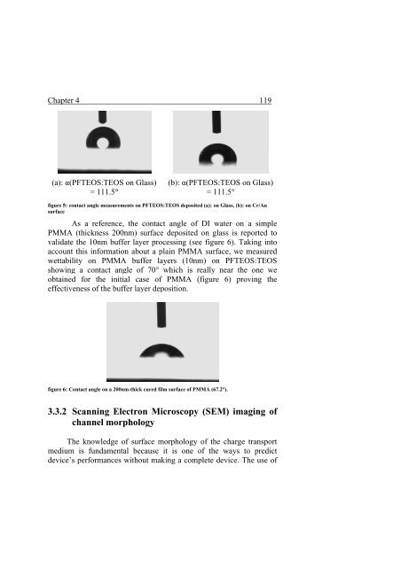
(a):<br />
(a): α(PFTEOS:TEOS (PFTEOS:TEOS (PFTEOS:TEOS on on Glass)<br />
Glass)<br />
= 111.5 111.5° °<br />
(b (b): ): α(PFTEOS:TEOS (PFTEOS:TEOS (PFTEOS:TEOS on on Glass)<br />
Glass)<br />
= 111.5° 111.5<br />
figure 55:<br />
contact contact angle angle measurements measurements on on P<br />
P PPFTEOS:TEOS<br />
FTEOS:TEOS FTEOS:TEOS deposited<br />
deposited (a): on on Glass,<br />
Glass, (b): (b): on on Cr/Au<br />
Cr/Au<br />
surface<br />
surface<br />
As As a a reference, reference, th<br />
th the e e contact contact angle angle of<br />
of DI DI water water on on a a simple<br />
simple<br />
PMMA PMMA (thickness (thickness 200nm) 200nm) surface surface deposited deposited on on glass glass is is reported reported to<br />
to<br />
validate validate the the 10nm 10nm buffer buffer layer layer processing processing (see<br />
(see figure figure 6). ). Taking Taking into<br />
into<br />
account account this this information information about about a a plain plain PMMA PMMA surface, surface, we we measured<br />
measured<br />
wettability wettability on on PMMA PMMA buffer buffer layers layers (10nm) (10nm) on on PFTEOS:TEOS<br />
PFTEOS:TEOS<br />
showing showing a a contact contact angle angle of of 70° 70° which which is is really really near near the the one one we<br />
we<br />
obtaine<br />
obtained d d for for the the initial initial case case of of PMMA PMMA (<br />
( (figure figure 6) ) proving proving the<br />
the<br />
effectiveness effectiveness of of the the buffer buffer layer layer deposition.<br />
deposition.<br />
figure 66:<br />
: : Contact Contact angle angl e e on on a a 200nm<br />
200nm-thick thick thick cured cured film film surface surface of PMMA (67.2°) .<br />
3.3.2<br />
3.3.2 Scanning Scanning Electron Electron Microscopy Microscopy (SEM) (SEM) imaging imaging of<br />
of<br />
channel channel morphology<br />
morphology<br />
The The knowledge knowledge of of surface surface morphology morphology of of the the charge charge transport<br />
transport<br />
medium medium is is fundamental fundamental because because it it is is one one of of the the ways ways to to predict<br />
predict<br />
device’s<br />
device’s performances performances without without making making a a complete complete device. device. T<br />
T TThe<br />
he he use use of<br />
of


