

tesi R. Miscioscia.pdf - EleA@UniSA
tesi R. Miscioscia.pdf - EleA@UniSA
tesi R. Miscioscia.pdf - EleA@UniSA

You also want an ePaper? Increase the reach of your titles
YUMPU automatically turns print PDFs into web optimized ePapers that Google loves.
Chapter 4 131<br />
Ea(eV)<br />
0.50<br />
0.45<br />
0.40<br />
0.35<br />
0.30<br />
0.25<br />
0.20<br />
0.15<br />
0.10<br />
PFTEOS:TEOS/PMMA 273nm<br />
PFTEOS:TEOS 270nm<br />
PMMA 115nm<br />
PMMA 225nm<br />
PMMA 400nm<br />
-20 -18 -16 -14 -12 -10 -8 -6 -4 -2<br />
V GS (V)<br />
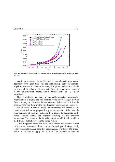
figure 15: Activation Energy (Ea(VGS)) graph for charge mobility in considered samples versus VGS<br />
gate bias.<br />
As it can be seen in figure 15, in every sample, activation energy<br />
decreases with gate bias but the relationship between sample’s<br />
physical features and activation energy appears unclear and all the<br />
curves tend to collapse, at high gate fields to a common value of<br />
0.12eV of activation energy and a precise trend of TMN is not<br />
identified.<br />
Our hypothesis is that a thermally-activated non-ideality<br />
phenomenon is hiding the real thermal behavior of charge mobility<br />
from our analysis. Between the main causes of device’s drift from the<br />
nominal behavior there are the gate leakages as we seen in chapter 3.<br />
Nevertheless it cannot easily be eliminated by means of the<br />
circuital equivalent we proposed in previous works [24] because the<br />
wide variation of mobility with gate field cannot be addressed in the<br />
model without losing the physical meaning of the extracted<br />
parameters. This is due to the introduction of an additional variable in<br />
the fitting of output curves in the triode region.<br />
Thus, it appears clear that we have to extract the channel current<br />
Ich from the measured drain current ID and gate leakage IG by<br />
following an alternative path. For these reasons we decided to change<br />
the approach and to apply the Esseni’s [26] method to clear the


