tesi R. Miscioscia.pdf - EleA@UniSA
tesi R. Miscioscia.pdf - EleA@UniSA
tesi R. Miscioscia.pdf - EleA@UniSA
You also want an ePaper? Increase the reach of your titles
YUMPU automatically turns print PDFs into web optimized ePapers that Google loves.
Gate-leakages 89<br />
The results are:<br />
= 35.4 nm Polyimide<br />
= 35.1 nm Polystyrene<br />
= 37.8 nm Resist<br />
These data do not show relevant differences in the films structure.<br />
3.3.2 Electrical characterization and device modeling<br />
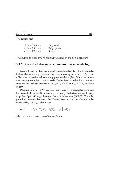
figure 6 shows that the output characteristics for the PI sample,<br />
before the annealing process, fail zero-crossing at VDS = 0 V. This<br />
effect can be attributed to a leaky gate insulator [10]. Moreover, since<br />
the sample revealed a symmetric Drain-Source behaviour, we can<br />
suppose the leakage current to be IS = ID = IG/2 at VDS = 0 V, as stated<br />
in [10].<br />
Plotting IS(VDS = 0 V) vs. VGS (see figure 4), a quadratic trend can<br />
be noticed. This result is common in many dielectric materials with<br />
trap-free Space-Charge Limited Current behaviour (SCLC). Thus the<br />
parasitic currents between the Drain contact and the Gate can be<br />
modeled by IG~VGD 2 obtaining:<br />
eq. 1 = −K<br />
( V −V<br />
)<br />
2<br />
2<br />
[ V −V<br />
] − V<br />
I S 2 GS T DS DS α DG<br />
where α can be named non-ideality factor.


