

tesi R. Miscioscia.pdf - EleA@UniSA
tesi R. Miscioscia.pdf - EleA@UniSA
tesi R. Miscioscia.pdf - EleA@UniSA

You also want an ePaper? Increase the reach of your titles
YUMPU automatically turns print PDFs into web optimized ePapers that Google loves.
Chapter 2 75<br />
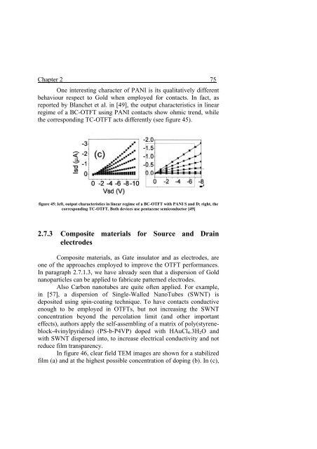
One interesting character of PANI is its qualitatively different<br />
behaviour respect to Gold when employed for contacts. In fact, as<br />
reported by Blanchet et al. in [49], the output characteristics in linear<br />
regime of a BC-OTFT using PANI contacts show ohmic trend, while<br />
the corresponding TC-OTFT acts differently (see figure 45).<br />
figure 45: left, output characteristics in linear regime of a BC-OTFT with PANI S and D; right, the<br />
corresponding TC-OTFT. Both devices use pentacene semiconductor [49]<br />
2.7.3 Composite materials for Source and Drain<br />
electrodes<br />
Composite materials, as Gate insulator and as electrodes, are<br />
one of the approaches employed to improve the OTFT performances.<br />
In paragraph 2.7.1.3, we have already seen that a dispersion of Gold<br />
nanoparticles can be applied to fabricate patterned electrodes.<br />
Also Carbon nanotubes are quite often applied. For example,<br />
in [57], a dispersion of Single-Walled NanoTubes (SWNT) is<br />
deposited using spin-coating technique. To have contacts conductive<br />
enough to be employed in OTFTs, but not increasing the SWNT<br />
concentration beyond the percolation limit (and other important<br />
effects), authors apply the self-assembling of a matrix of poly(styreneblock-4vinylpyridine)<br />
(PS-b-P4VP) doped with HAuCl4.3H2O and<br />
with SWNT dispersed into, to increase electrical conductivity and not<br />
reduce film transparency.<br />
In figure 46, clear field TEM images are shown for a stabilized<br />
film (a) and at the highest possible concentration of doping (b). In (c),


