

tesi R. Miscioscia.pdf - EleA@UniSA
tesi R. Miscioscia.pdf - EleA@UniSA
tesi R. Miscioscia.pdf - EleA@UniSA

You also want an ePaper? Increase the reach of your titles
YUMPU automatically turns print PDFs into web optimized ePapers that Google loves.
60 State of the Art<br />
it is important to remember the Halik and Klauk paper published in<br />
2005 on Nature [36] in which a SAM dielectric of only 2.5 nm is<br />
inserted in a benchmark structure, bottom-gate top contacts, made on<br />
silicon wafers.<br />
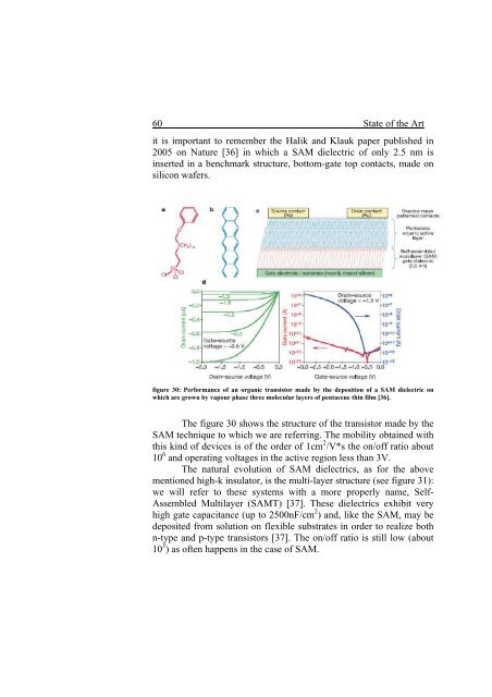
figure 30: Performance of an organic transistor made by the deposition of a SAM dielectric on<br />
which are grown by vapour phase three molecular layers of pentacene thin film [36].<br />
The figure 30 shows the structure of the transistor made by the<br />
SAM technique to which we are referring. The mobility obtained with<br />
this kind of devices is of the order of 1cm 2 /V*s the on/off ratio about<br />
10 6 and operating voltages in the active region less than 3V.<br />
The natural evolution of SAM dielectrics, as for the above<br />
mentioned high-k insulator, is the multi-layer structure (see figure 31):<br />
we will refer to these systems with a more properly name, Self-<br />
Assembled Multilayer (SAMT) [37]. These dielectrics exhibit very<br />
high gate capacitance (up to 2500nF/cm 2 ) and, like the SAM, may be<br />
deposited from solution on flexible substrates in order to realize both<br />
n-type and p-type transistors [37]. The on/off ratio is still low (about<br />
10 3 ) as often happens in the case of SAM.


