

tesi R. Miscioscia.pdf - EleA@UniSA
tesi R. Miscioscia.pdf - EleA@UniSA
tesi R. Miscioscia.pdf - EleA@UniSA

Create successful ePaper yourself
Turn your PDF publications into a flip-book with our unique Google optimized e-Paper software.
Chapter 4 123<br />
mobility with the dimension of grains and thus of grain boundaries as<br />
Horowitz et Al. [3] have shown for thiophenes and also in previous<br />
works. The analysis of mobility curves versus gate bias (gate voltagedependent<br />
mobility) has been performed for PMMA samples and<br />
extended for a 225nm PMMA insulator treated in CF4 plasma and<br />
subsequently in PFTEOS:TEOS and a bufferized<br />
PFTEOS:TEOS/PMMA sample.<br />
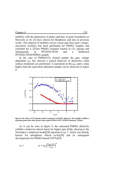
In the case of PMMA/CF4 treated sample the gate voltage<br />
dependent µFE has showed a typical behavior of dielectrics when<br />
surface treatments are performed. A maximum in the µFE and a value<br />
higher than the equivalent untreated sample can be observed in figure<br />
8.<br />
μ (cm 2 /Vs)<br />
0.20<br />
0.15<br />
0.10<br />
0.05<br />
0.00<br />
-0.05<br />
-20 -15 -10 -5 0 5<br />
V G (V)<br />
figure 8: the effect of CF4 plasma surface treatment on PMMA dielectric. The mobility exhibits a<br />
maximum point and values greater than a plain PMMA OTFT. (PMMA thickness: 225nm)<br />
As it can be seen in figure 8, the untreated PMMA dielectric<br />
exhibits a behavior almost linear for higher gate fields, obeying to the<br />
Necliudov’s empirical model[28] reported in eq. 3 which was already<br />
known for amorphous silicon (a-Si)[30] and its subsequent<br />
developments for PMMA-based OTFTs[29].<br />
eq. 3 <br />
<br />
<br />
<br />
PMMA 225nm<br />
PMMA 225nm - CF4


