

tesi R. Miscioscia.pdf - EleA@UniSA
tesi R. Miscioscia.pdf - EleA@UniSA
tesi R. Miscioscia.pdf - EleA@UniSA

Create successful ePaper yourself
Turn your PDF publications into a flip-book with our unique Google optimized e-Paper software.
74 State of the Art<br />
2.7.2.2 Polyaniline<br />
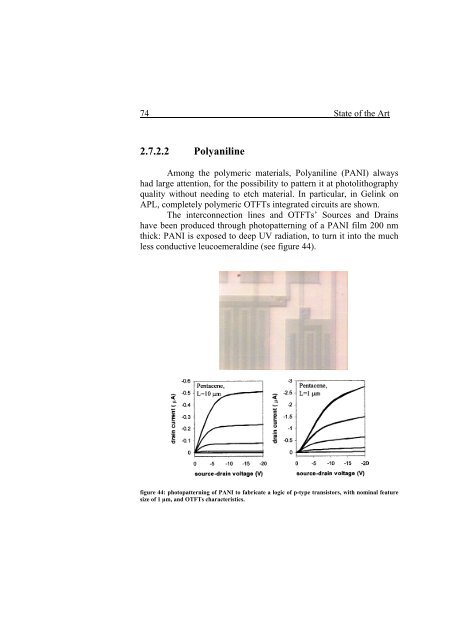
Among the polymeric materials, Polyaniline (PANI) always<br />
had large attention, for the possibility to pattern it at photolithography<br />
quality without needing to etch material. In particular, in Gelink on<br />
APL, completely polymeric OTFTs integrated circuits are shown.<br />
The interconnection lines and OTFTs’ Sources and Drains<br />
have been produced through photopatterning of a PANI film 200 nm<br />
thick: PANI is exposed to deep UV radiation, to turn it into the much<br />
less conductive leucoemeraldine (see figure 44).<br />
figure 44: photopatterning of PANI to fabricate a logic of p-type transistors, with nominal feature<br />
size of 1 µm, and OTFTs characteristics.


