

tesi R. Miscioscia.pdf - EleA@UniSA
tesi R. Miscioscia.pdf - EleA@UniSA
tesi R. Miscioscia.pdf - EleA@UniSA

Create successful ePaper yourself
Turn your PDF publications into a flip-book with our unique Google optimized e-Paper software.
Gate-leakages 91<br />
It has to be considered that the increase of gate current is<br />
provoked by a complete overlap between contacts and gate and a<br />
relatively small gate-source and gate-drain separation (in the figure 5<br />
it has to be 1.000µm (insulator) + 65nm (pentacene) = 1.065 µm)<br />
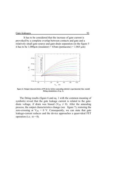
figure 6: Output characteristics of PI device before annealing (dotted: experimental; line: model<br />
fitting simulations of eq. 1).<br />
The fitting results (figure 6 and eq. 1 with the common meaning of<br />
symbols) reveal that the gate leakage current is related to the gatedrain<br />
voltage, if drain was biased (VDS ≠ 0). After the annealing<br />
process, the output characteristics change (see figure 7), restoring the<br />
zero-crossing at VDS = 0 V. Consequently, we can state that gate<br />
leakage-current reduces and the device approaches a quasi-ideal FET<br />
operation (i.e.: α = 0).


