

tesi R. Miscioscia.pdf - EleA@UniSA
tesi R. Miscioscia.pdf - EleA@UniSA
tesi R. Miscioscia.pdf - EleA@UniSA

You also want an ePaper? Increase the reach of your titles
YUMPU automatically turns print PDFs into web optimized ePapers that Google loves.
Chapter 2 63<br />
materials, the higher is the current passing through the junction itself.<br />
Thus, for p-type transistor, the contact is much better as the WF of the<br />
contact approaches the semiconductor HOMO level (in which we<br />
would like to inject holes).<br />
Many p-type materials have HOMO levels that require, for the<br />
adequate holes injection, high work-function electrodes to minimize<br />
the interface barrier. For example, for p-type pentacene based<br />
transistors, it will be sufficient to use metals such as gold, nickel,<br />
platinum, etc. to realize the appropriate source and drain contacts (see<br />
table 1).<br />
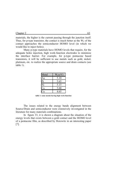
Metal WF(eV)<br />
Au 5.10<br />
Pt 5.65<br />
Ni 5.15<br />
Co 5.00<br />
Cu 4.65<br />
table 1: some metals having high work-function<br />
The issues related to the energy bands alignment between<br />
Source/Drain and semiconductor were extensively investigated in the<br />
literature for many materials combinations.<br />
In figure 33, it is shown a diagram about the situation of the<br />
energy levels that exists between a gold contact and the HOMO level<br />
of a pentacene film, as described by Horowitz in an interesting paper<br />
[7].


