

tesi R. Miscioscia.pdf - EleA@UniSA
tesi R. Miscioscia.pdf - EleA@UniSA
tesi R. Miscioscia.pdf - EleA@UniSA

Create successful ePaper yourself
Turn your PDF publications into a flip-book with our unique Google optimized e-Paper software.
92 Chapter 3<br />
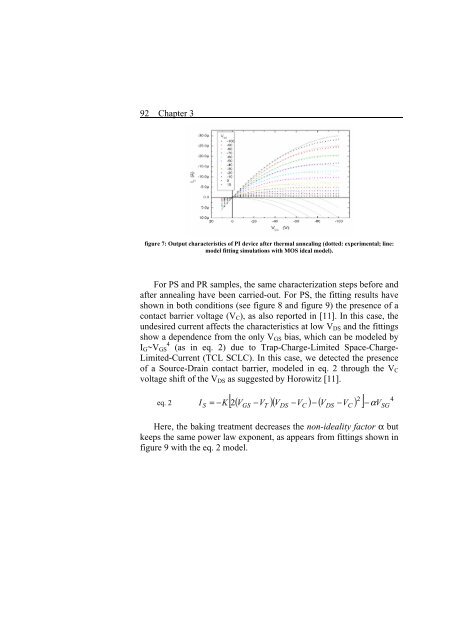
figure 7: Output characteristics of PI device after thermal annealing (dotted: experimental; line:<br />
model fitting simulations with MOS ideal model).<br />
For PS and PR samples, the same characterization steps before and<br />
after annealing have been carried-out. For PS, the fitting results have<br />
shown in both conditions (see figure 8 and figure 9) the presence of a<br />
contact barrier voltage (VC), as also reported in [11]. In this case, the<br />
undesired current affects the characteristics at low VDS and the fittings<br />
show a dependence from the only VGS bias, which can be modeled by<br />
IG~VGS 4 (as in eq. 2) due to Trap-Charge-Limited Space-Charge-<br />
Limited-Current (TCL SCLC). In this case, we detected the presence<br />
of a Source-Drain contact barrier, modeled in eq. 2 through the VC<br />
voltage shift of the VDS as suggested by Horowitz [11].<br />
2 4<br />
[ ] − V<br />
eq. 2 = −K<br />
( V −V<br />
)( V −V<br />
) − ( V −V<br />
)<br />
I S 2 GS T DS C DS C α SG<br />
Here, the baking treatment decreases the non-ideality factor α but<br />
keeps the same power law exponent, as appears from fittings shown in<br />
figure 9 with the eq. 2 model.


