

tesi R. Miscioscia.pdf - EleA@UniSA
tesi R. Miscioscia.pdf - EleA@UniSA
tesi R. Miscioscia.pdf - EleA@UniSA

You also want an ePaper? Increase the reach of your titles
YUMPU automatically turns print PDFs into web optimized ePapers that Google loves.
126 Exceptions in morphology-mobility relationship<br />
Also in this case the enhanced structural order of the first<br />
pentacene monolayers in comparison to the plain sample evidences a<br />
general increase of the charge transport and mobility and a peak value<br />
at VGS=-11V as it has already been shown for CF4 in figure 8 and<br />
references [31].<br />
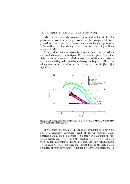
Finally, if we compare mobility results obtained for treated and<br />
untreated dielectrics as in figure 12, and extract grain dimensions<br />
statistics from channel’s SEM images, a relationship between<br />
maximum mobility and channel morphology can be graphically shown<br />
taking also into account values extracted in previous works [24][23] in<br />
figure 13.<br />
μ (cm 2 /Vs)<br />
0.2<br />
0.1<br />
0.0<br />
-21 -14 -7 0 7<br />
V G (V)<br />
PMMA 115nm<br />
PMMA 225nm<br />
PMMA 420nm<br />
PMMA 225nm - CF4<br />
PFTEOS:TEOS/PMMA<br />
PFTEOS:TEOS<br />
figure 12: gate voltage dependent mobility comparison for PMMA, PMMA/CF4, PFTEOS:TEOS<br />
and PFTEOS:TEOS/PMMA devices<br />
If we observe the figure 13 (black square symbols), it’s possible to<br />
notice a generally increasing trend of charge mobility versus<br />
pentacene lateral grain dimension. This behavior is common in large<br />
grains semiconductors[3] and the limiting factor is not the grain<br />
mobility but, according to the back-to-back Schottky schematization<br />
of the grain-to-grain interface, the current flowing through a grain<br />
boundary at room temperature is limited by thermionic emission. (eq.<br />
4).


