

tesi R. Miscioscia.pdf - EleA@UniSA
tesi R. Miscioscia.pdf - EleA@UniSA
tesi R. Miscioscia.pdf - EleA@UniSA

You also want an ePaper? Increase the reach of your titles
YUMPU automatically turns print PDFs into web optimized ePapers that Google loves.
76 State of the Art<br />
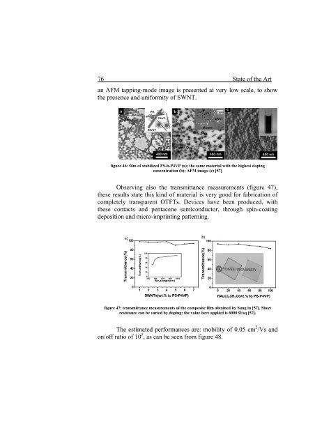
an AFM tapping-mode image is presented at very low scale, to show<br />
the presence and uniformity of SWNT.<br />
figure 46: film of stabilized PS-b-P4VP (a); the same material with the highest doping<br />
concentration (b); AFM image (c) [57]<br />
Observing also the transmittance measurements (figure 47),<br />
these results state this kind of material is very good for fabrication of<br />
completely transparent OTFTs. Devices have been produced, with<br />
these contacts and pentacene semiconductor, through spin-coating<br />
deposition and micro-imprinting patterning.<br />
figure 47: transmittance measurements of the composite film obtained by Sung in [57]. Sheet<br />
resistance can be varied by doping; the value here applied is 6000 Ω/sq [57].<br />
The estimated performances are: mobility of 0.05 cm 2 /Vs and<br />
on/off ratio of 10 5 , as can be seen from figure 48.


