Superconducting Technology Assessment - nitrd
Superconducting Technology Assessment - nitrd
Superconducting Technology Assessment - nitrd

Create successful ePaper yourself
Turn your PDF publications into a flip-book with our unique Google optimized e-Paper software.
For this study, the readiness of the system integration technologies required by RSFQ was evaluated. The major<br />
conclusions are:<br />
■<br />
■<br />
■<br />
■<br />
The design of secondary packaging technologies (e.g., boards, MCMs, 3-D packaging)<br />
and interconnects (e.g., cables, connectors) for SCE chips is technically feasible and fairly<br />
well understood.<br />
The lack of a superconducting packaging foundry with matching design and fabrication<br />
capabilities is a major issue.<br />
The technology for the refrigeration plant needed to cool large systems, along with the<br />
associated mechanical and civil infrastructure, is understood well enough to allow technical<br />
and cost estimates to be made.<br />
Testing of a superconducting supercomputer has not been fully addressed yet. Testing<br />
mostly addressed modular approaches at cold temperatures by providing standard physical<br />
interfaces and limited functional testing at high frequencies.<br />
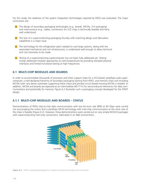
6.1 MULTI-CHIP MODULES AND BOARDS<br />
In order to accommodate thousands of processor and other support chips for a SCE-based, petaflops-scale supercomputer,<br />
a well-designed hierarchy of secondary packaging starting from RSFQ and memory chips and including<br />
MCMs (with very dense substrates supporting these chips) and printed circuit boards housing MCMs is needed. In<br />
addition, MCMs and boards are expected at an intermediate (40-77 K) for semiconductor electronics for data communications<br />
and potentially for memory. Figure 6.2 illustrates such a packaging concept developed for the HTMT<br />
design.<br />
6.1.1 MULTI-CHIP MODULES AND BOARDS – STATUS<br />
Demonstrations of RSFQ chip-to-chip data communication with low bit error rate (BER) at 60 Gbps were carried<br />
out encouraging the notion that a petaflops MCM technology with inter-chip communication at the clock rate of<br />
the chips is feasible (Figure 6.3). However, these demonstrations were carried out on very simple MCM-D packages<br />
with superconducting inter-chip connections, fabricated in an R&D environment.<br />
Figure 6-2. HTMT conceptual packaging for cryogenic processing and data communications.<br />
114