- Page 1 and 2:
SUPERCONDUCTING TECHNOLOGY ASSESSME
- Page 3 and 4:
Summary of Findings The STA conclud
- Page 5 and 6:
CHAPTER 02: ARCHITECTURAL CONSIDERA
- Page 7 and 8:
CHAPTER 06: SYSTEM INTEGRATION 6.1
- Page 9 and 10:
INDEX OF FIGURES CHAPTER 01: INTROD
- Page 11 and 12:
APPENDIX G: ISSUES AFFECTING RSFQ C
- Page 13 and 14:
CONTENTS OF CD EXECUTIVE SUMMARY CH
- Page 15 and 16:
LIMITATIONS OF CURRENT TECHNOLOGY C
- Page 17 and 18:
State of the Industry Today, expert
- Page 19 and 20:
01 This document presents the resul
- Page 21 and 22:
1.2 LIMITATIONS OF CONVENTIONAL TEC
- Page 23 and 24:
1.3.2 RSFQ ATTRIBUTES Important att
- Page 25 and 26:
The end point of this roadmap defin
- Page 27 and 28:
CRYOGENIC ENVIRONMENT High-speed ne
- Page 29 and 30:
■ ■ Chalmers University in Swed
- Page 31 and 32:
Random Access Memory Options Random
- Page 33 and 34:
Compact Package Feasible Thousands
- Page 35 and 36:
The major issue to be addressed wil
- Page 37 and 38:
02 No radical execution paradigm sh
- Page 39 and 40:
The key challenges at the processor
- Page 41 and 42:
2.2 MICROPROCESSORS - CURRENT STATU
- Page 43 and 44:
2.2.3 CORE1 BIT-SERIAL MICROPROCESS
- Page 45 and 46:
Potential Problems The initial vers
- Page 47 and 48:
The microarchitecture of supercondu
- Page 49 and 50:
2.5 MICROPROCESSORS - CONCLUSIONS A
- Page 51:
2.7 MICROPROCESSORS - FUNDING In th
- Page 54 and 55:
SUPERCONDUCTIVE RSFQ PROCESSOR AND
- Page 56 and 57:
3.1 RSFQ PROCESSORS The panel devel
- Page 58 and 59:
TABLE 3.1-1. PUBLISHED SUPERCONDUCT
- Page 60 and 61:
S G G Chip-side microstrip S Carrie
- Page 62 and 63:
3.1.3 RSFQ PROCESSORS - ROADMAP The
- Page 64 and 65:
3.1.5 RSFQ PROCESSORS - ISSUES AND
- Page 66 and 67:
Since these memory concepts are so
- Page 68 and 69:
Simulations show that the input int
- Page 70 and 71:
SFQ RAM Status The results of five
- Page 72 and 73:
Investment for SFQ Memory The inves
- Page 74 and 75:
4MB MRAM BIT CELL: 1 MTJ & 1 TRANSL
- Page 76 and 77:
The roadmap identifies early analyt
- Page 78 and 79:
MRAM Major Issues and Concerns Mate
- Page 80 and 81:
3.3 CAD TOOLS AND DESIGN METHODOLOG
- Page 82 and 83:
Issues and Concerns Present simulat
- Page 84 and 85:
Investment The investment estimated
- Page 87 and 88:
04 By 2010 production capability fo
- Page 89 and 90:
Table 4-1 summarizes the roadmap fo
- Page 91 and 92:
4.1 SCE IC CHIP MANUFACTURING - SCO
- Page 93 and 94:
Significant activity in the area of
- Page 95 and 96:
4.3 SCE CHIP FABRICATION FOR HEC -
- Page 97 and 98:
The superconductive IC chip fabrica
- Page 99 and 100:
Table 4-6 shows how gate speed depe
- Page 101 and 102:
Parameter spreads in superconductiv
- Page 103 and 104:
TABLE 4-9. SCALING REQUIREMENTS FOR
- Page 105 and 106:
ELEMENT 2006 2007 2008 2009 2010 Pi
- Page 107 and 108:
A potential savings of ~40% in the
- Page 109 and 110:
05 Packaging and chip-to-chip inter
- Page 111 and 112:
TABLE 5-1. I/O TECHNOLOGIES FOR PET
- Page 113 and 114:
For further discussions of the opti
- Page 115 and 116:
5.1.3 OPTICAL INTERCONNECT TECHNOLO
- Page 117 and 118:
In this case, an optical receiver w
- Page 119 and 120:
Examples of what has been achieved
- Page 121 and 122:
5.3.4 OUTPUT: 4 K RSFQ TO ROOM TEMP
- Page 123 and 124:
Figure 5-4. Superconducting 16x16 c
- Page 125 and 126:
06 The design of secondary packagin
- Page 127 and 128:
For this study, the readiness of th
- Page 129 and 130:
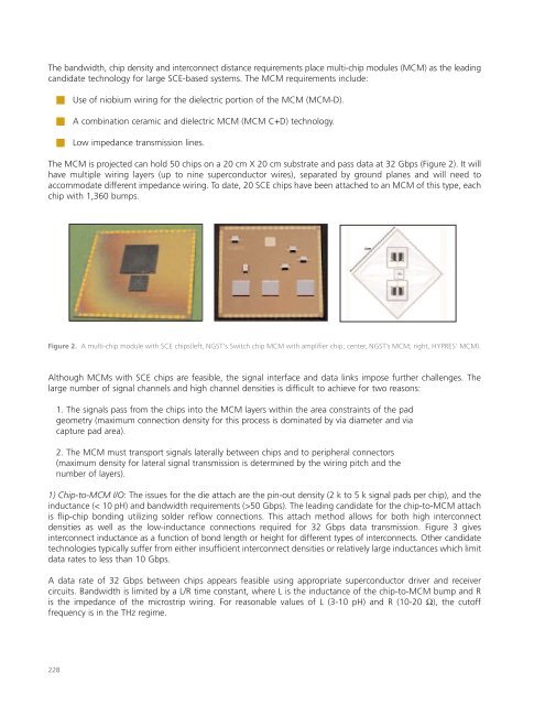
6.1.3 MULTI-CHIP MODULES AND BOARDS
- Page 131 and 132:
TABLE 6-2. MCM FABRICATION TOOLS AN
- Page 133 and 134:
6.2.3. 3-D PACKAGING - ISSUES AND C
- Page 135 and 136:
Several companies have demonstrated
- Page 137 and 138:
In selecting the cooling approach f
- Page 139 and 140:
Another issue is the cost of the re
- Page 141 and 142:
Some of the thermal and electrical
- Page 143 and 144:
Optical interconnects may require t
- Page 145 and 146:
6.6.4 SYSTEM INTEGRITY AND TESTING
- Page 147 and 148:
Appendix A
- Page 149 and 150:
■ ■ ■ ■ Construct a detaile
- Page 151 and 152:
Appendix B
- Page 153 and 154:
GOVERNMENT George Cotter Director f
- Page 155 and 156:
Appendix C
- Page 157 and 158:
TERMS/DEFINITIONS IHEC LLNL JJ JPL
- Page 159 and 160:
Appendix D
- Page 161 and 162:
The time-dependent behavior of this
- Page 163 and 164:
RSFQ electronics is faster and diss
- Page 165 and 166:
Similar to CMOS, the irreducible po
- Page 167 and 168:
Appendix E
- Page 169 and 170:
The report further identified four
- Page 171 and 172:
Analog high temperature superconduc
- Page 173 and 174:
Appendix F
- Page 175 and 176:
Only one significant effort to arch
- Page 177 and 178:
Execution Models Organizing hardwar
- Page 179 and 180:
Development Issues and Approaches T
- Page 181 and 182:
Appendix G
- Page 183 and 184:
The two-junction comparator, the ba
- Page 185 and 186:
Bias Currents A major cause of degr
- Page 187 and 188:
Power and bias current Power is dis
- Page 189 and 190: Appendix H
- Page 191 and 192: SMT MRAM Another direct selection s
- Page 193 and 194: Speed and Density The first planned
- Page 195 and 196: 120 0.10 100 Write I (mA) 0.08 0.06
- Page 197 and 198: Appendix I
- Page 199 and 200: Table 1 Representative Nb and NbN-B
- Page 201 and 202: ground plane may be located either
- Page 203 and 204: Table 5 Reactive Ion Etch Parameter
- Page 205 and 206: Table 6 Junction Array Summary of T
- Page 207 and 208: shorts in the first wiring layer we
- Page 209 and 210: B. Yield Yield measurements are an
- Page 211 and 212: RSFQ logic will eventually find wid
- Page 213 and 214: [47] B. Bumble, H. G. LeDuc, J. A.
- Page 215 and 216: Appendix J
- Page 217 and 218: Fig. 2. The Schematic View describe
- Page 219 and 220: Fig. 4. The VHDL View captures the
- Page 221 and 222: Fig. 6. LMeter is specialized softw
- Page 223 and 224: Fig. 8. Layout-versus-Schematic ver
- Page 225 and 226: Appendix K
- Page 227 and 228: 1. CURRENT STATUS OF OPTICAL INTERC
- Page 229 and 230: 1.2. CURRENT OPTICAL INTERCONNECT R
- Page 231 and 232: If technology, power, or cost limit
- Page 233 and 234: 3.4 COARSE VS. DENSE WAVE DIVISION
- Page 235 and 236: 3.5 DEVELOPMENTS FOR LOW TEMPERATUR
- Page 237 and 238: 5. ROADMAP The roadmap below shows
- Page 239: Appendix L
- Page 243 and 244: While using short flex cables is th
- Page 245 and 246: We must note that the reparability
- Page 247 and 248: Intermediate Temperature stage Disp
- Page 249 and 250: Small Cryocoolers Among commercial
- Page 251 and 252: Although cooling of the 4 K circuit
- Page 253 and 254: Supplying DC current to all of the
- Page 255 and 256: These properties enable the possibi
- Page 257: For additional copies, please conta