Superconducting Technology Assessment - nitrd
Superconducting Technology Assessment - nitrd
Superconducting Technology Assessment - nitrd

You also want an ePaper? Increase the reach of your titles
YUMPU automatically turns print PDFs into web optimized ePapers that Google loves.
3.1.6 RSFQ PROCESSORS – PROJECTED FUTURE CAPABILITY<br />
Chip density is a major factor in the ultimate success of RSFQ technology in HEC, and in many other nascent applications.<br />
Comparing present 1-µm RSFQ technology with 0.25-µm CMOS that has many more wiring layers, the panel can draw<br />
general conclusions about RSFQ density limits. As described further in Chapter 4, the last Northrop Grumman process could<br />
be extended to 1 million JJs/cm 2 in one year with a few readily achievable improvements in the fabrication process.<br />
This does not imply that 1 million JJs/cm 2 is the limit of RSFQ technology; greater density would be achieved from<br />
further advances in fabrication, design, and innovative concepts. For example, self-clocked circuits without bias<br />
resistors is one concept that would reduce power and eliminate the separate clock distribution circuitry, thereby<br />
reducing clock jitter and increasing gate density. The panel foresees multi-level circuit fabrication multiplying the functionality<br />
of chips as another step forward.<br />
3.2 MEMORY<br />
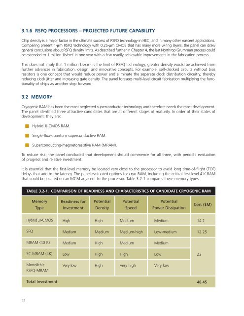
Cryogenic RAM has been the most neglected superconductor technology and therefore needs the most development.<br />
The panel identified three attractive candidates that are at different stages of maturity. In order of their states of<br />
development, they are:<br />
■<br />
■<br />
■<br />
Hybrid JJ-CMOS RAM.<br />
Single-flux-quantum superconductive RAM.<br />
<strong>Superconducting</strong>-magnetoresistive RAM (MRAM).<br />
To reduce risk, the panel concluded that development should commence for all three, with periodic evaluation<br />
of progress and relative investment.<br />
It is essential that the first-level memory be located very close to the processor to avoid long time-of-flight (TOF)<br />
delays that add to the latency. The panel evaluated options for cryo-RAM, including the critical first-level 4 K RAM<br />
that could be located on an MCM adjacent to the processor. Table 3.2-1 compares these memory types.<br />
TABLE 3.2-1. COMPARISON OF READINESS AND CHARACTERISTICS OF CANDIDATE CRYOGENIC RAM<br />
Memory<br />
Type<br />
Readiness for<br />
Investment<br />
Potential<br />
Density<br />
Potential<br />
Speed<br />
Potential<br />
Power Dissipation<br />
Cost ($M)<br />
Hybrid JJ-CMOS<br />
High<br />
High<br />
Medium<br />
Medium<br />
14.2<br />
SFQ<br />
Medium<br />
Medium<br />
Medium-high<br />
Low-medium<br />
12.25<br />
MRAM (40 K)<br />
Medium<br />
High<br />
Medium<br />
Medium<br />
SC-MRAM (4K)<br />
Low<br />
High<br />
High<br />
Low<br />
22<br />
Monolithic<br />
RSFQ-MRAM<br />
Very low<br />
High<br />
Very high<br />
Very low<br />
Total Investment<br />
48.45<br />
52