Superconducting Technology Assessment - nitrd
Superconducting Technology Assessment - nitrd
Superconducting Technology Assessment - nitrd

You also want an ePaper? Increase the reach of your titles
YUMPU automatically turns print PDFs into web optimized ePapers that Google loves.
All IC chips on completed wafers undergo room temperature testing prior to dicing. Process control monitor (PCM)<br />
chips are mounted on superconductive multi-chip modules (MCMs) tested at 4 K. These Nb-based MCMs are produced<br />
in the main fabrication facility, while MCMs for product IC chips are produced separately. (MCM fabrication and<br />
testing is discussed in Chapter 6.)<br />
The fabrication group:<br />
■<br />
■<br />
■<br />
■<br />
Maintains a database of PCM data and is responsible for its analysis, which provides<br />
the basis for the process design rules.<br />
Maintains the gate library, which is developed in collaboration with the circuit design<br />
group(s); is responsible for incorporating circuit designs into mask layouts and for<br />
procuring photolithographic masks.<br />
Produces IC chips for verification of CAD, gates, designs, IC chip architectures, and all<br />
IC chips required for the demonstrations associated with this program.<br />
Potentially can provide foundry services for other digital SCE programs (government,<br />
academic, or commercial).<br />
4.2 DIGITAL SUPERCONDUCTIVE IC CHIP FABRICATION – STATUS<br />
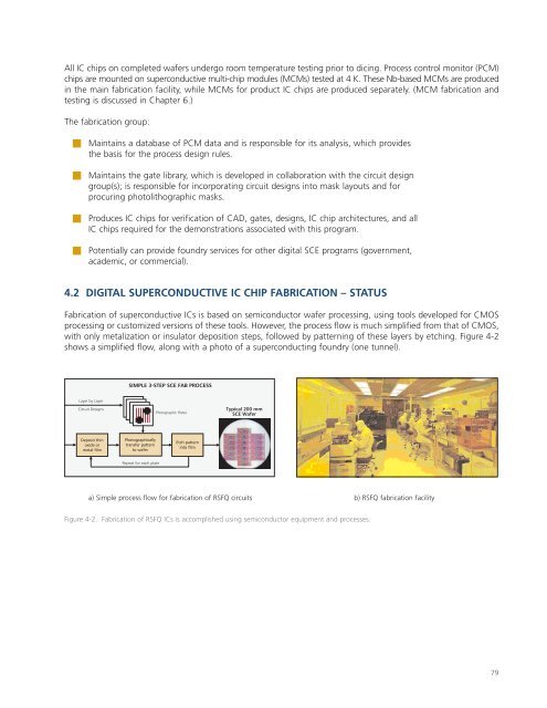
Fabrication of superconductive ICs is based on semiconductor wafer processing, using tools developed for CMOS<br />
processing or customized versions of these tools. However, the process flow is much simplified from that of CMOS,<br />
with only metalization or insulator deposition steps, followed by patterning of these layers by etching. Figure 4-2<br />
shows a simplified flow, along with a photo of a superconducting foundry (one tunnel).<br />
SIMPLE 3-STEP SCE FAB PROCESS<br />
Layer by Layer<br />
Circuit Designs<br />
Photographic Plates<br />
Typical 200 mm<br />
SCE Wafer<br />
Deposit thin<br />
oxide or<br />
metal film<br />
Photographically<br />
transfer pattern<br />
to wafer<br />
Etch pattern<br />
into film<br />
Repeat for each plate<br />
a) Simple process flow for fabrication of RSFQ circuits b) RSFQ fabrication facility<br />
Figure 4-2. Fabrication of RSFQ ICs is accomplished using semiconductor equipment and processes.<br />
79