Superconducting Technology Assessment - nitrd
Superconducting Technology Assessment - nitrd
Superconducting Technology Assessment - nitrd

Create successful ePaper yourself
Turn your PDF publications into a flip-book with our unique Google optimized e-Paper software.
Inter-chip Communications<br />
Driver and receiver circuits have already been demonstrated to 60 Gbps per line in the NG fabrication processes. Since<br />
speed and bit error rate (BER) will improve as J C increases, the circuit technology is ready now. The principal task will be<br />
to accommodate the increased number of high-data-rate lines on each chip and MCM. Shrinking bump size and minimum<br />
spacing, better design tools, and simulation models will be important to minimize reflections and cross-talk at<br />
both the signal and ground chip-to-MCM bumps. The crossbar switch program provides a rich experience base in the<br />
engineering of ribbon cables. In particular, the trade-off between heat leak and signal loss is well understood.<br />
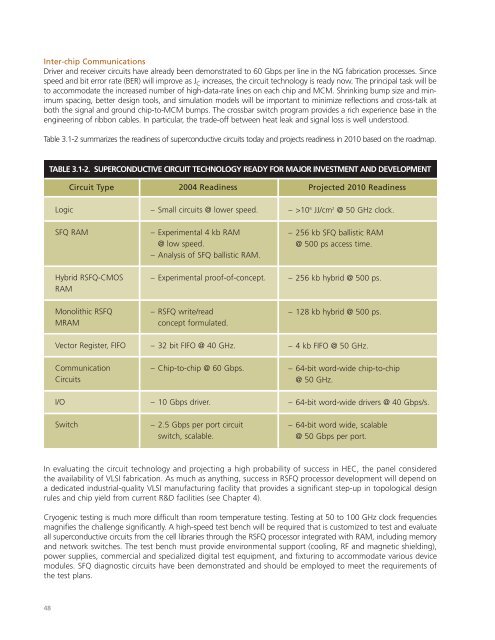
Table 3.1-2 summarizes the readiness of superconductive circuits today and projects readiness in 2010 based on the roadmap.<br />
TABLE 3.1-2. SUPERCONDUCTIVE CIRCUIT TECHNOLOGY READY FOR MAJOR INVESTMENT AND DEVELOPMENT<br />
Circuit Type<br />
2004 Readiness<br />
Projected 2010 Readiness<br />
Logic<br />
– Small circuits @ lower speed.<br />
– >10 6 JJ/cm 2 @ 50 GHz clock.<br />
SFQ RAM<br />
– Experimental 4 kb RAM<br />
@ low speed.<br />
– Analysis of SFQ ballistic RAM.<br />
– 256 kb SFQ ballistic RAM<br />
@ 500 ps access time.<br />
Hybrid RSFQ-CMOS<br />
RAM<br />
– Experimental proof-of-concept.<br />
– 256 kb hybrid @ 500 ps.<br />
Monolithic RSFQ<br />
MRAM<br />
– RSFQ write/read<br />
concept formulated.<br />
– 128 kb hybrid @ 500 ps.<br />
Vector Register, FIFO<br />
– 32 bit FIFO @ 40 GHz.<br />
– 4 kb FIFO @ 50 GHz.<br />
Communication<br />
Circuits<br />
– Chip-to-chip @ 60 Gbps.<br />
– 64-bit word-wide chip-to-chip<br />
@ 50 GHz.<br />
I/O<br />
– 10 Gbps driver.<br />
– 64-bit word-wide drivers @ 40 Gbps/s.<br />
Switch<br />
– 2.5 Gbps per port circuit<br />
switch, scalable.<br />
– 64-bit word wide, scalable<br />
@ 50 Gbps per port.<br />
In evaluating the circuit technology and projecting a high probability of success in HEC, the panel considered<br />
the availability of VLSI fabrication. As much as anything, success in RSFQ processor development will depend on<br />
a dedicated industrial-quality VLSI manufacturing facility that provides a significant step-up in topological design<br />
rules and chip yield from current R&D facilities (see Chapter 4).<br />
Cryogenic testing is much more difficult than room temperature testing. Testing at 50 to 100 GHz clock frequencies<br />
magnifies the challenge significantly. A high-speed test bench will be required that is customized to test and evaluate<br />
all superconductive circuits from the cell libraries through the RSFQ processor integrated with RAM, including memory<br />
and network switches. The test bench must provide environmental support (cooling, RF and magnetic shielding),<br />
power supplies, commercial and specialized digital test equipment, and fixturing to accommodate various device<br />
modules. SFQ diagnostic circuits have been demonstrated and should be employed to meet the requirements of<br />
the test plans.<br />
48