Superconducting Technology Assessment - nitrd
Superconducting Technology Assessment - nitrd
Superconducting Technology Assessment - nitrd

Create successful ePaper yourself
Turn your PDF publications into a flip-book with our unique Google optimized e-Paper software.
SMT MRAM<br />
SMT MRAM has only one read/write current path and can yield much higher densities than FS-TMR. A nanomagnetic<br />
bit has recently been demonstrated. Cornell University, NIST, and Freescale have demonstrated that pulse<br />
current densities of 10 7 -10 8 A/cm 2 can rotate the magnetic polarization at 40 K and switching times decrease from<br />
5 ns to ~600 ps at high pulse amplitudes. SMT switching is most effective for single magnetic domains, ideal for<br />
bits smaller than ~300 nm. Present SMT structures rely on GMR with low MR, but higher MR materials that will<br />
reduce the switching current and time have been identified. A 2-Ω, 90-nm device was simulated to switch at 0.1<br />
mA, equivalent to a voltage bias of 0.2 mV, and a simulated device switched in 50 ps.<br />
SMT memory may be more compatible with RSFQ logic than FS devices, but it is even more embryonic and<br />
considerable effort will be required to optimize the materials and cell architectures. It should be emphasized, however,<br />
that the opportunity afforded by combining MRAM with superconductive circuits would remain unexplored unless<br />
it is funded by government investment for this ultra-high performance computing niche.<br />
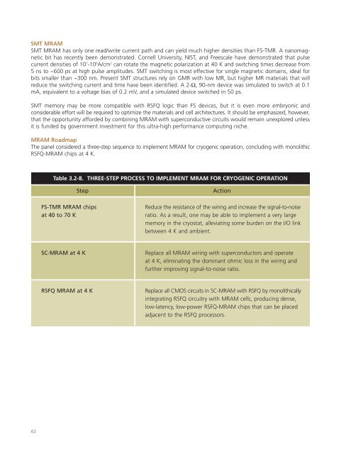
MRAM Roadmap<br />
The panel considered a three-step sequence to implement MRAM for cryogenic operation, concluding with monolithic<br />
RSFQ-MRAM chips at 4 K.<br />
Table 3.2-8. THREE-STEP PROCESS TO IMPLEMENT MRAM FOR CRYOGENIC OPERATION<br />
Step<br />
FS-TMR MRAM chips<br />
at 40 to 70 K<br />
Action<br />
Reduce the resistance of the wiring and increase the signal-to-noise<br />
ratio. As a result, one may be able to implement a very large<br />
memory in the cryostat, alleviating some burden on the I/O link<br />
between 4 K and ambient.<br />
SC-MRAM at 4 K<br />
Replace all MRAM wiring with superconductors and operate<br />
at 4 K, eliminating the dominant ohmic loss in the wiring and<br />
further improving signal-to-noise ratio.<br />
RSFQ MRAM at 4 K<br />
Replace all CMOS circuits in SC-MRAM with RSFQ by monolithically<br />
integrating RSFQ circuitry with MRAM cells, producing dense,<br />
low-latency, low-power RSFQ-MRAM chips that can be placed<br />
adjacent to the RSFQ processors.<br />
62