Superconducting Technology Assessment - nitrd
Superconducting Technology Assessment - nitrd
Superconducting Technology Assessment - nitrd

Create successful ePaper yourself
Turn your PDF publications into a flip-book with our unique Google optimized e-Paper software.
In summary, several ideas have been studied. In two of these, the memory cells were the NEC vortex transitional<br />
(VT) type cells, which were developed for use with voltage-state logic and require voltage-state drivers. One design<br />
provided for SFQ input and output pulses on a 256-bit array with potential for high speed. However, scaled to<br />
64 kb, this array would have untenable power dissipation and large size. The other group did not demonstrate a<br />
complete system.<br />
The cryo-RAM (CRAM) developed at HYPRES had attractive estimated access and cycle times for 4-kb blocks, but<br />
no high-speed data. The estimates for power and access and cycle times scaled to 64-kb are attractive. Circuit<br />
density and cycle and access times would be more favorable with increased current density. The ballistic RAM<br />
(BRAM) is an interesting concept that will require more research. For all, more advanced fabrication would lead<br />
to greater circuit density.<br />
SFQ RAM Readiness for Investment<br />
Although SFQ RAM technology is not as advanced as hybrid CMOS, the panel feels that very attractive concepts<br />
exist and should be investigated to support RSFQ processors for HEC. An effort should be made to further evaluate<br />
the CRAM and BRAM in order to project their advantages and disadvantages and to quantify power, access time,<br />
density, and probability of success. The panel urges that the better choice be pursued at least to the bit-slice stage<br />
to further define the key parameters. If successful, the development should be completed.<br />
SFQ RAM Projections<br />
The CRAM design should be scaled to a 20 kA/cm 2 process and 64-kb RAM to determine the important parameters<br />
of speed, power, and chip size. The BRAM concept will require more design evaluation to determine its potential,<br />
but either of these ideas could have advantages over the hybrid Josephson-CMOS memory in speed and power.<br />
As noted for the hybrid memory, memory chip design will require close collaboration between the architecture and<br />
memory teams in order to find the best processor-memory communication and internal memory chip organization<br />
to meet the read/write latency, access cycle time, and bandwidth requirements of 50 GHz processors.<br />
SFQ RAM Issues and Concerns<br />
As in any large RSFQ circuit, margins and flux trapping may be problems. The testing of the CRAM was only done<br />
at low speed, so new issues may arise when operated at high speed. In the present DRO BRAM concept, methods<br />
for refreshing will have to be explored in order to retain the beneficial aspects of this memory.<br />
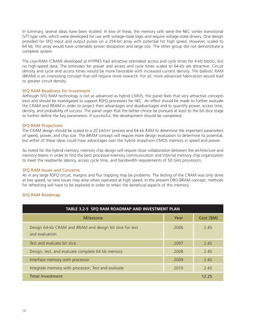
SFQ RAM Roadmap<br />
TABLE 3.2-5 SFQ RAM ROADMAP AND INVESTMENT PLAN<br />
Milestone Year Cost ($M)<br />
Design 64-kb CRAM and BRAM and design bit slice for test<br />
and evaluation<br />
Test and evaluate bit slice<br />
Design, test, and evaluate complete 64 kb memory<br />
Interface memory with processor<br />
Integrate memory with processor; Test and evaluate<br />
Total Investment<br />
2006<br />
2007<br />
2008<br />
2009<br />
2010<br />
2.45<br />
2.45<br />
2.45<br />
2.45<br />
2.45<br />
12.25<br />
58